 Fraunhofer Institute for Electronic Nano Systems
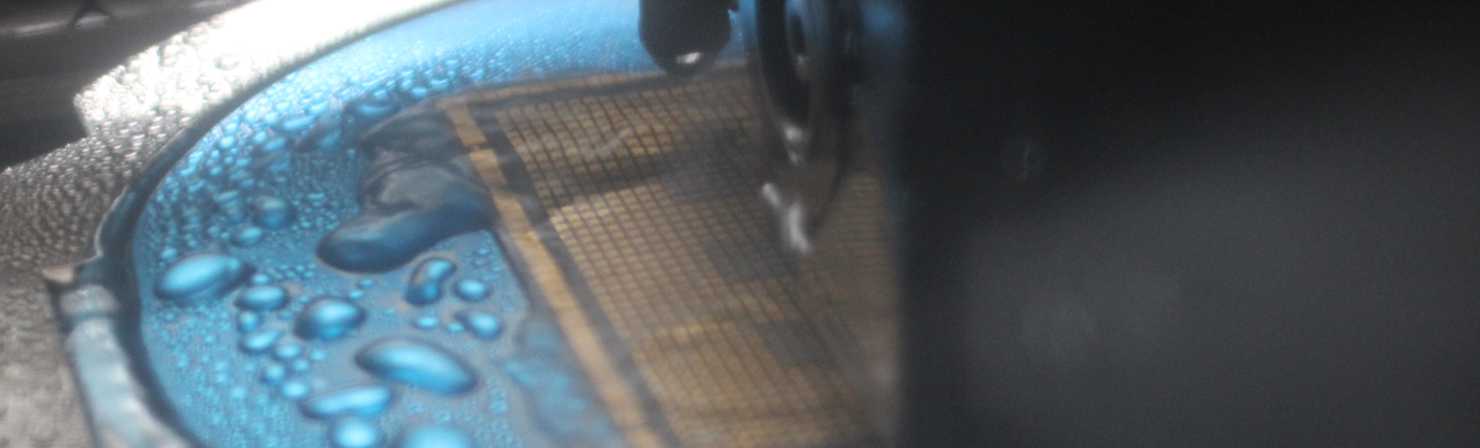
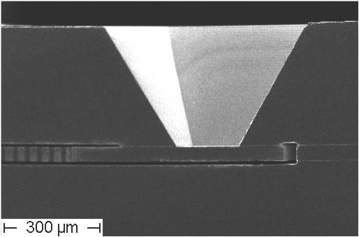
One of the last processes in line is the dicing process, where whole wafers are separated into single chips. Special dicing blades, coated with different diamond-based powder enable the high precision dicing with small width and low edge deformation (chipping). Two DISCO dicing machines are available for research, development and prototyping - the semi automatic DAD-2HTM and the automatic DFD6340.
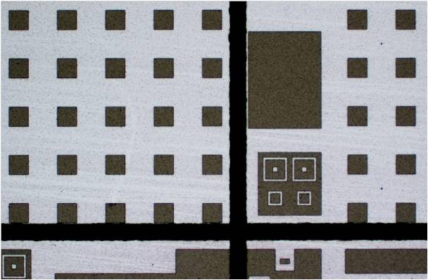
Materials like silicon, glass, ceramics, and metals can be diced into small chips. Depending on the material and the application different dicing blades are used. The thickness of such a blade defines the dicing width and blades from 15 µm up to 500 µm can be used. The maximum substrate thickness is around 4 mm.
Materials
- Silicon
- Glass
- Metals
- Ceramics
- Bonded wafers (Si-Glass, Glass-Glass, Si-Si)
Process steps
- Taping the wafers on dicing tape (adhesive, thermal, UV-tape)
- Surface protection by taping if needed
- Vacuum chucking and alignment
- Programming of the dicing recipe
- Automatic dicing process
Parameters
- Dicing blades: 2“... 3“
- Substrate thickness: up to 4 mm
- Alignment accuracy: 1...2 µm
- Dicing line width: 15...500 µm