 Fraunhofer Institute for Electronic Nano Systems
Interview
Parylene – an all-rounder: Ultra-thin polymer with protective properties
If sounds seem increasingly muffled, if the outside world is getting quieter by the day, and if conversations become difficult to follow, especially when there is a lot of background noise, these are likely the initial stages of hearing loss. If left untreated, these early signs of hearing loss can lead to becoming completely deaf. Cochlear implants offer hope to people with severe hearing loss and deaf people to take a more active role in everyday life and access the world of sound. Current research efforts are focused on making progress in the field of technically assisted auditory perception with the aid of cochlear implants, which should enable improved speech intelligibility while at the same time ensuring a high level of patient comfort. The polymer Parylene, the innovative key component of these developments, is a real all-rounder, providing virtually invisible protection for the necessary electronics. At Fraunhofer ENAS, researchers such as Franz Selbmann are working on using this wafer-thin polymer to shield sensitive electronics for medical engineering and industry from external influences. In this interview, the scientist explains what makes Parylene unique and the potential applications of this advanced material, for instance for new generations of medical implants.
Mr. Selbmann, at Fraunhofer ENAS you are carrying out extensive research into the material Parylene. Can you explain exactly what Parylene is and how the material is produced?
Parylene, its full name being poly(para-xylylene), is an interesting material and belongs to the group of polymers. It is produced by a process known as chemical vapor deposition (CVD). This layer deposition process involves depositing the material from the gas phase in a vacuum chamber at room temperature on various substrates, such as silicon wafers, with an extremely thin layer thickness, homogeneously and stress-free. The resulting layer is fully 3D compliant. This means that even geometrically demanding substrates with unusual topographies and filigree structures can be coated and every last corner, every sharp edge, every tiny pore and every cavity of the initial substrate can be completely and homogeneously covered with a Parylene layer.
What is it about this polymer that makes it so unusual and special?
The material has unique technical properties that make it interesting for a wide range of applications in medicine, electronics and the semiconductor industry.
The outstanding capabilities of Parylene are particularly evident in the medical and healthcare sectors: Its biocompatibility and biostability make the material particularly well adapted to biological processes, making it ideal for use in the human body as an enclosure for miniaturized systems and aids. As a result, no pathological interactions occur, no allergies, irritations or defense reactions are triggered and no particles or toxic substances are released in combination with body fluids that could pose a health risk, even if they remain in the body permanently. This ensures greater patient safety and well-being.
The polymer is also extremely resistant. As it is non-reactive with other chemical substances, in other words “inert,” it is ideal for use in harsh environments. Thanks to this chemical inertness, it remains completely intact and stable even when it comes into contact with corrosive or aggressive reactants such as acids, bases and solvents.
Its barrier properties also allow, for example, encapsulated electronics to be effectively protected against aggressive ambient conditions and make it impossible for gases, chemicals or other liquids to penetrate.
The polymer is also dielectric. This property is particularly useful for insulating electrically conductive materials or electronic components.
Last but not least, Parylene is characterized by its optical transparency. This means that light can pass freely through the polymer, making it attractive for optical applications such as LED protection.
What are the potential applications for the polymer in which these outstanding properties can be utilized?
This combination of properties makes the polymer the ideal candidate for encapsulating, coating, sealing and refining electronic and mechanical components, as well as surfaces and entire systems across a wide range of industries. Whether in the automotive, aerospace, optics and microelectronics, chemical, or medical industries, Parylene is already widely used.
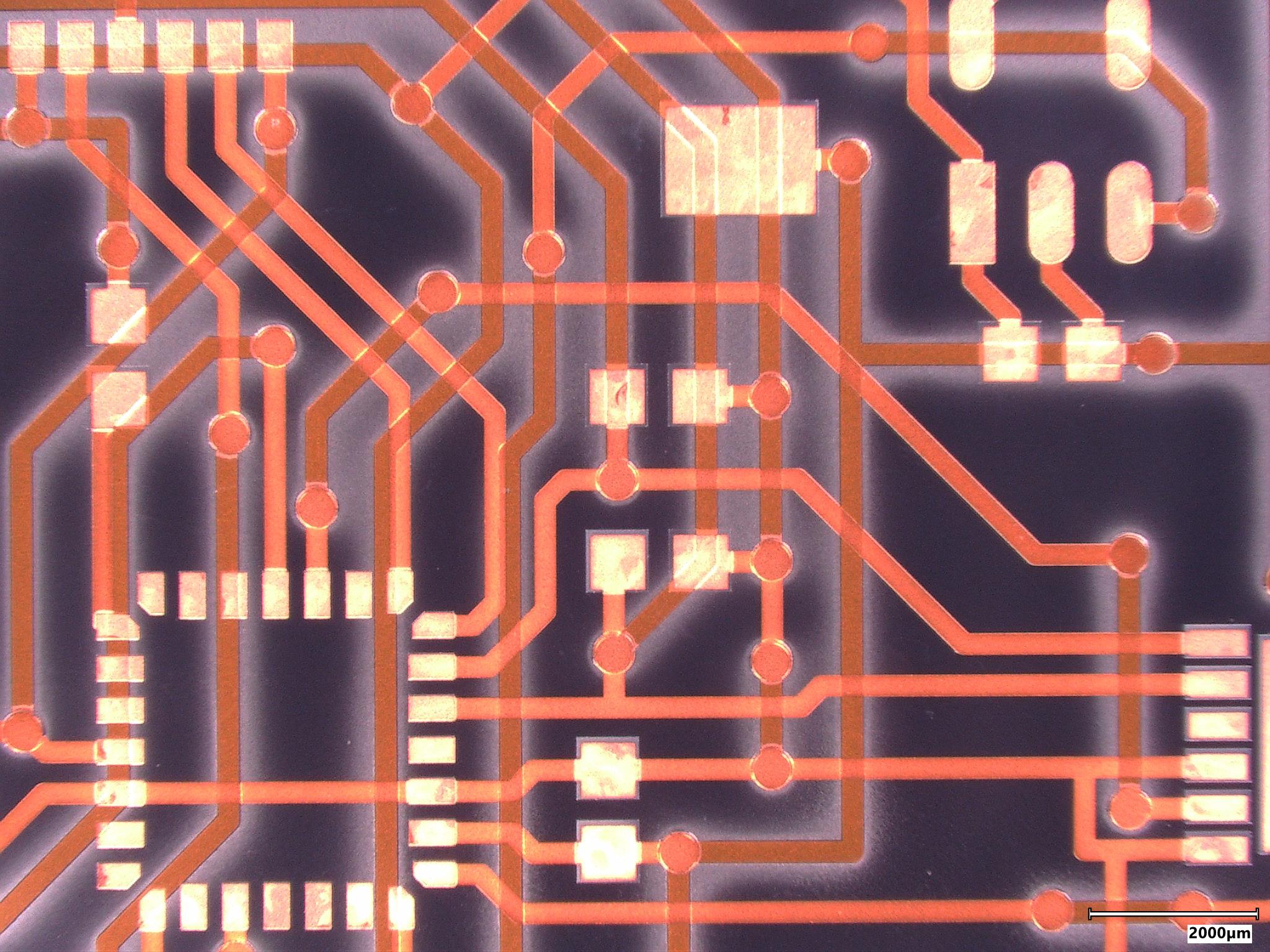
One of the main applications of Parylene is encapsulation to provide printed circuit boards, for example, with corrosion protection against salt and moisture using a thin Parylene film, thus ensuring that systems can continue to function.
At Fraunhofer ENAS, we are also investigating the suitability of Parylene as an adhesive for use in microtechnological bonding processes, in which the polymer can be used as an adhesive or bonding layer at chip and wafer level with a high mechanical strength. Due to its excellent temperature resistance, which allows it to withstand higher temperatures, the polymer has already been successfully utilized in the field of assembly and connection technology in microelectronics and microsystems technology to establish a new bonding process based on Parylene.
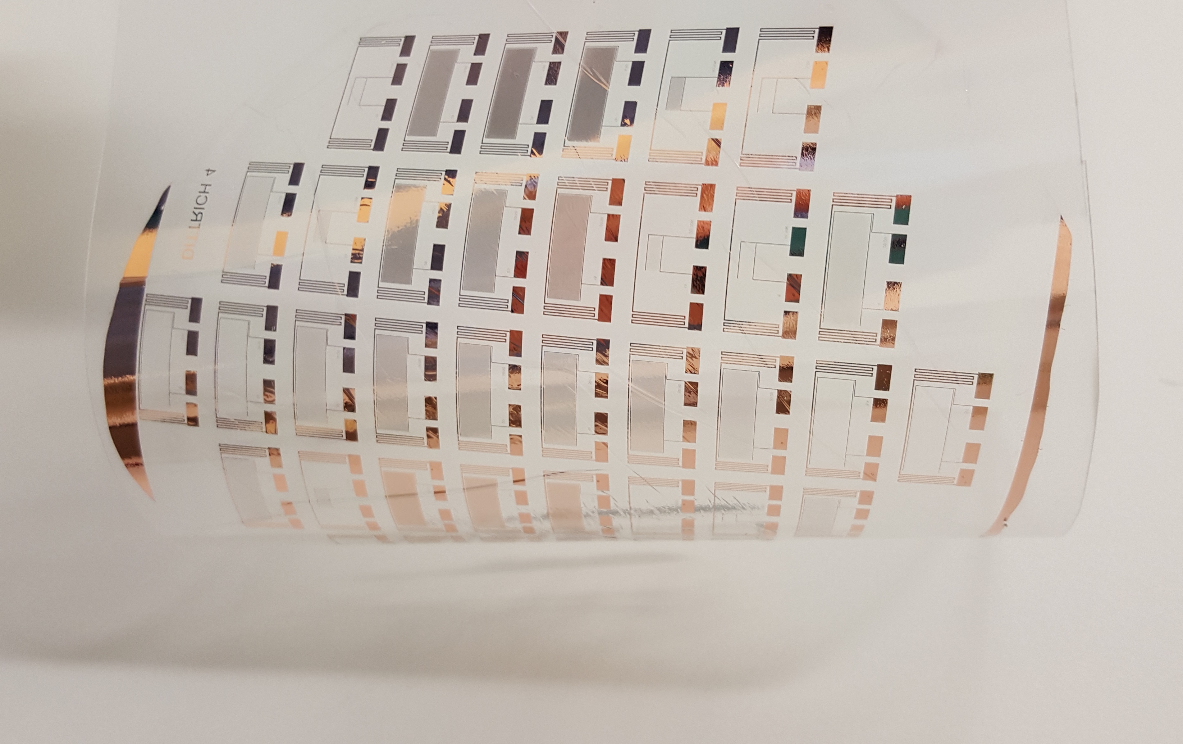
We are also researching how ultra-thin, flexible printed circuit boards can be produced using Parylene. For this purpose, the polymer is deposited on a wafer and equipped with metallic conductor tracks. With a thickness of 20 micrometers, the resulting Parylene-based printed circuit board is 10 times thinner than previous commercially available printed circuit boards. In this way, wearables can be produced that are worn close to the body, for example in the form of smart medical patches that can be used to continuously monitor vital parameters. We can also see potential applications in the field of “geometry-adaptive sensors” and the monitoring of lightweight structures. These ultra-thin Parylene-based printed circuit boards could be integrated into the wings of airplanes, for example, as carriers for corresponding sensors and could thus monitor sensitive parameters that provide indications of material fatigue and wear. The light weight of the sensor system does not affect the statics and stability of the aircraft wings. This means that materials can be replaced ahead of time before a serious hazard arises.
You mentioned that Parylene is biocompatible, which makes it particularly attractive for applications in the medical sector. What specific areas of applications do you have in mind for the healthcare sector?
If, for example, a patient's heart is no longer beating at the correct rate, a pacemaker may be needed to restore the correct beat. These often comprise a titanium housing that carries the necessary and sensitive electronics. The use of Parylene, which coats and encapsulates all of the electronics as a protective layer, could eliminate the need for a titanium housing and thus create opportunities for further miniaturization of pacemakers and other medical implants, making them significantly smaller and lighter than previous systems.
Some patients also notice a slight “bulging” of the skin at the implantation site after a pacemaker has been inserted into the body, which is caused by the titanium housing. A Parylene-encapsulated system that adapts better to the body would ensure improved wearing comfort.
Parylene-based coatings and encapsulations for electronics therefore offer enormous potential not only when it comes to pacemakers, but also for entirely new generations of medical implants, which in future will be able to operate without additional housings. As the example outlined at the beginning of this article shows, Parylene is being utilized to bring about progress in the field of hearing prosthetics. What exactly are you working on?
We are working together with various partners in the “SEMECO” future cluster to make cochlear implants not only smaller and lighter, but also smarter going forward, thus giving patients with hearing loss or deafness hope for a better quality of life. The idea is to record brain activity signals, which serve as an indicator of attentiveness, perception and speech comprehension, in order to tailor the implant to the individual. In this way, background noise can be suppressed while the auditory focus is directed to specific sounds, such as those of conversational partners.
Within the scope of this research work, we are developing a highly miniaturized and biocompatible encapsulation method for the implant based on Parylene. The combination of different layers is intended to create an “ultra-barrier.” This is designed not only to protect the integrated sensors and components of the inner ear implant from bodily fluids, but also to protect the human organism from harmful substances from the technical system. What's more, the combination of layers acts as an electromagnetic shield for the sensitive high-performance circuits, guaranteeing optimum protection without having to rely on a conventional housing. The use of Parylene makes it possible to significantly reduce the size of the complex implant, making it easier to insert into the body and improving both patient and wearing comfort.
Thank you very much, Mr. Selbmann, for this interview and for giving us an insight into Parylene, the “all-rounder.”
Please do not hesitate to contact us if you would like to find out more about Parylene or if you have any questions about the many different applications for this plastic.
Last modified: