 Fraunhofer Institute for Electronic Nano Systems
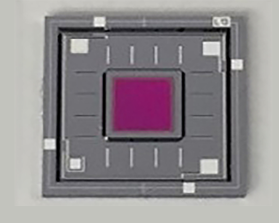
This technology platform enables the three-dimensional structuring of silicon wafers using wet and dry etching processes in various combinations. The structuring steps for further layers are embedded in this process sequence, such as e.g. SiO2 and Si3N4 layers for electrical insulation, metallic layers for electrical contacting or dielectric layers for optically active areas.
Precise cavities are etched for electrostatically controlled or capacitive detecting MEMS/MOEMS. Elastic elements (springs) for preferably vertical movements are created by a combination of at least two Si etching processes. The combination of a wet etching process (setting a defined spring thickness) and a DRIE etching process (definition of lateral dimensions) enables a high degree of effectiveness while at the same time realizing complex and precise spring geometries.
The assembly of the pre-processed wafers is carried out by means of wafer-level bonding technologies, wherein currently preferably direct bonding, anodic bonding or adhesive bonding by means of SU-8 or parylene layers are applied.
The technology platform is currently established on a 6" wafer size and is constantly being improved. Main applications are optical filters for the wavelength range from the visible (VIS) to the near infrared (NIR) to the mid-infrared (MIR). Furthermore, passive 3-dimensional shapes Si components are fabricated.