 Fraunhofer Institute for Electronic Nano Systems
Press Release
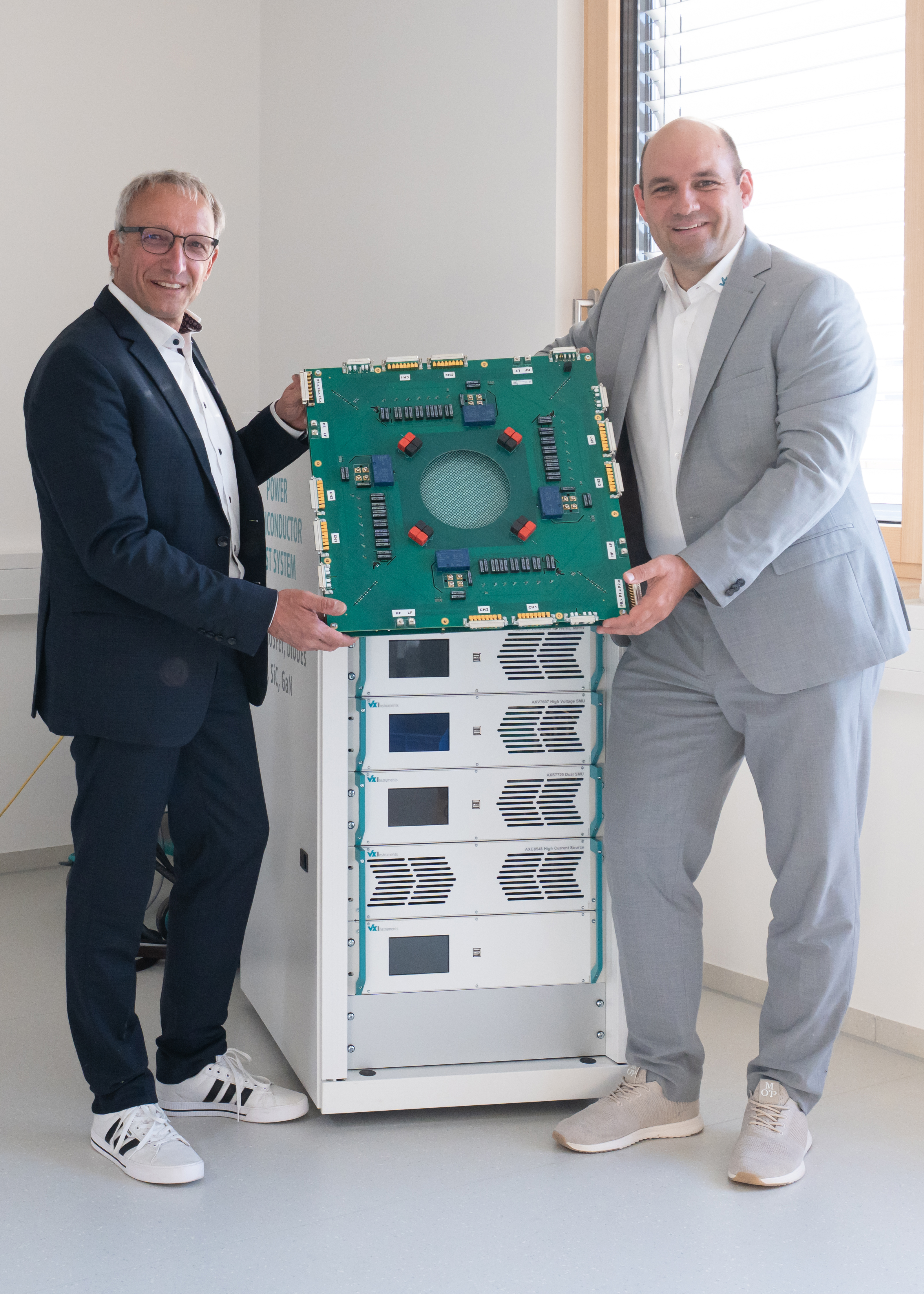
Fraunhofer ENAS and VX Instruments Collaborate on Revolutionary Testing System to Address Critical Technological Gap in SiC- and GaN-Based Semiconductor Innovations
The increasing use of electric vehicles and renewable energy sources is one of the main drivers of dynamics in the semiconductor market. This has led to growing demand for power semiconductors such as silicon carbide (SiC) and gallium nitride (GaN), which are considered key to advancements in power electronics and thus to the success of the transport and energy transition. To ensure the highest quality levels for SiC- and GaN-based chip innovations, the Fraunhofer Institute for Electronic Nano Systems ENAS and VX Instruments GmbH are developing a cutting-edge, future-oriented, and highly efficient testing system. By performing precise, parallel functional tests at the wafer level, the system will enable the production of high-performance, extremely robust, and stable devices for power electronics applications while reducing testing times and costs. The system’s combination of complex testing processes and artificial intelligence will significantly increase the efficiency of semiconductor manufacturing.

Semiconductor devices based on SiC and GaN are ideal for demanding power applications due to their unique physical and electrical properties. Their high thermal stability, excellent thermal conductivity, high efficiency at high power densities, resistance to high voltages, and long lifespan make them particularly attractive for power electronics as well as for use in electric mobility and modern energy supply networks.
As part of their collaboration within the European Test and Reliability Center (ETRC) – Europe’s new competence center for testing complex semiconductor technologies – Fraunhofer ENAS and VX Instruments GmbH are developing an innovative solution for testing SiC- and GaN-based power semiconductors with their novel system.
The resulting testing technology will enable high-precision, parallel testing of semiconductor devices, which will significantly improve quality, shorten testing times, and increase test throughputs.
Effective testing of power semiconductors at wafer level enhances sustainability in semiconductor manufacturing
“The key breakthrough in the testing technology that we are developing in collaboration with VX Instruments GmbH lies in its ability to enable testing of SiC and GaN semiconductor devices directly at the wafer level and with complete test coverage – combined with unprecedented speed, efficiency, and precision. At present, quality and functionality testing does not take place until a relatively late stage in the manufacturing process, after power semiconductor devices have already been assembled into complex power electronic modules using assembly and connection technology. Identifying defects at this stage makes testing extremely costly. Our innovative functional testing solution starts much earlier in the value chain, enabling SiC and GaN wafers to be inspected for weak points and defects before the semiconductor modules are even assembled. In addition to reducing the material reject rate, increasing resource efficiency, and enhancing sustainability in manufacturing, it will result in a significant reduction in testing costs,” explains Prof. Dr. Harald Kuhn, Institute Director at Fraunhofer ENAS, highlighting the advantages of the new semiconductor testing process.
The jointly developed testing system also enables highly parallel wafer-level testing, allowing multiple semiconductor devices to be tested simultaneously in a single step. This results in significantly shorter testing times and enhances the efficiency of the entire manufacturing process.
“By inspecting devices based on SiC and GaN power semiconductors at the wafer level, our new testing solution closes an important gap that existed up until now in the field of semiconductor testing. Not only does it serve as an important link in the successful development and rollout of innovative products in the rapidly growing power electronics market, but it also represents a revolutionary step toward sustainable energy supply and environmentally friendly mobility," says Prof. Dr. Harald Kuhn.
New testing system combines static and dynamic testing of SiC and GaN power semiconductors in a single system
Since weak points and defects, such as dislocations in the SiC and GaN crystals, can have a significant impact on the material properties and hence the functionality of the semiconductor material, comprehensive testing of various semiconductor parameters at an early stage of the manufacturing process is critical for ensuring the stability of the modules that will be deployed in power electronics. The new functional test developed by the two partners enables early and comprehensive testing of both static and dynamic semiconductor parameters, such as on-state resistance, switching characteristics, and short-circuit behavior, with the advantage that only a single system is required. By conducting wafer-level inspections of SiC and GaN semiconductor devices, the system ensures that only flawless and fully functional devices – meeting the highest standards of quality and reliability – proceed to the subsequent stage in the semiconductor manufacturing process.
Applying artificial intelligence to accelerate defect detection
The functional testing of semiconductor devices generates vast amounts of test data, which need to be evaluated as quickly as possible to provide rapid feedback to the manufacturing process and enable timely intervention if faults and defects should be detected. “To accelerate this step, we are working together with Fraunhofer ENAS to shorten the evaluation time for this test data, which will speed up testing processes. This is made possible by integrating machine learning methods and artificial intelligence into our new semiconductor testing system. By identifying weak points at an early stage, semiconductor manufacturers will be able to ensure that only defect-free and fully functional power semiconductors proceed to the next stages in manufacturing processes and are assembled into complex modules. This will pave the way for high-quality and reliable innovations in semiconductor technologies,” explains Christian Degenhart, CEO of VX Instruments GmbH, summarizing the advantages of the new testing solution developed in collaboration with Fraunhofer ENAS.
The highly efficient system for testing power semiconductor devices at the wafer level, developed by Fraunhofer ENAS and VX Instruments GmbH, will expand the range of services provided by the recently opened European Test and Reliability Center (ETRC) allowing it to offer innovative test procedures to its customers.
About the European Test and Reliability Center
The European Test and Reliability Center (ETRC) at Fraunhofer ENAS is the only competence center of its kind in Europe for testing the quality and reliability of future semiconductor innovations. With its state-of-the-art testing infrastructure, in-depth expertise, and strong network of partners from science and industry, the ETRC will provide comprehensive solutions for assessing the quality, functionality, and longevity of pioneering microtechnologies. The ETRC’s portfolio of services includes both the research and development of new test and evaluation methods as well as the optimization of these new methods for specific applications. In addition, the ETRC will offer comprehensive services for the verification of small batches as well as practical advice for businesses. A specialist program will also provide dedicated training and further education for specialists in testing procedures and reliability assessments. www.enas.fraunhofer.de/etrc
About VX Instruments GmbH
VX Instruments GmbH (VXI), based in Landshut, Bavaria, Germany, was founded in 1989 by Johann Degenhart as Ingenieurbüro Johann Degenhart. Since then, VXI has grown to become a recognized specialist for high-precision semiconductor testing systems and electronic measurement instruments – with customers in over 30 countries worldwide. With over 30 years of experience in measurement technology, VXI supplies high-end solutions for the products of tomorrow – including applications in the automotive industry, semiconductor manufacturing, and renewable energies. VX Instruments’ systems combine exceptional engineering and expertise in interdisciplinary applications with an outstanding isolated design that enables the highest precision at maximum speed. Around 500 systems with VX Instruments’ technology are in use worldwide – often in 24-hour continuous operation without compromising on measurement accuracy. VXI’s testing systems support both front-end and back-end testing and continue to set new standards, particularly in the field of power semiconductors. www.vxinstruments.com
About Fraunhofer ENAS
The Fraunhofer Institute for Electronic Nano Systems’ key strength lies in the holistic development of “intelligent systems” for various applications. Its research activities range from the development of innovative wafer and packaging technologies to the production of electronic components, micro- and nano sensors, and actuators, as well as developing system concepts and system integration technologies, including communication interfaces. Fraunhofer ENAS uses state-of-the-art and AI-supported test and reliability methods to transfer the developed solutions into practical applications. The institute guides customer projects from the initial idea through to the design phase, technology development or implementation using existing technologies, to the final tested prototype.
Images available for download at
https://datas.weichertmehner.com/ENAS_VXInstruments.zip
Use for media free of charge
Image credits: ©VX Instruments GmbH
Last modified: