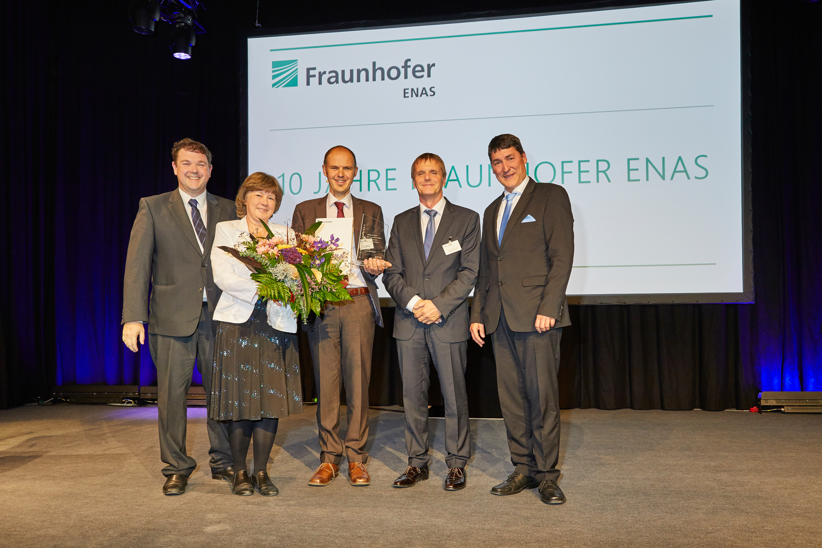
Fraunhofer ENAS honored the development of technologies for 3D integration in MEMS applications with the Fraunhofer ENAS Research Award
Dr. Lutz Hofmann received the research award of Fraunhofer ENAS in 2018. With his research results on 3D integration and copper-filled through silicon vias in microsystems, he contributed to the expert status of the Fraunhofer Institute for Electronic Nano Systems ENAS in Chemnitz as one of the few research institutes in this field.

The research award of the Fraunhofer Institute for Electronic Nano Systems ENAS, endowed with 5,000 euros, was awarded to Dr. Lutz Hofmann in 2018. The scientist and engineer from Chemnitz investigates technologies that are required for three-dimensional integration (3D integration) into micro-electromechanical systems (MEMS). With the help of these integration technologies, MEMS can be integrated into modules and systems that exhibit a high degree of miniaturization or particularly thin form factors.
With his work, Lutz Hofmann has helped the Fraunhofer ENAS in Chemnitz to achieve expert status in the special research field of through silicon vias (TSV) for microsystems. The renowned market analyst Yole Développement lists the Chemnitz Institute as one of three European research institutes in this field, alongside the notable French research institute CEA-Leti and the Belgian IMEC, and as one of only six worldwide.
With his dissertation »3D-Wafer Level Packaging approaches for MEMS by using Cu-based High Aspect Ratio Through Silicon Vias« Dr. Hofmann received his doctorate in 2017 at Chemnitz University of Technology. In 2015, he has already received an award for the best conference publication with a publication on the topic of 3D integration at the “International Wafer Level Packaging Conference (IWLPC)” in San Jose, USA.
The Fraunhofer ENAS Research Award honors the outstanding results in the development of various TSV-based technology concepts for the creation of 3D packages for MEMS at wafer level. The comprehensive treatment of both detailed individual processes and process sequences and the comparative, application-oriented development of various technology approaches are particularly noteworthy, as are the results for the integration of very thin MEMS, e.g. for smartcard/chipcard applications.
Within the scope of his research work, Dr. Hofmann established an extensive network of cooperation with external partners from industry and research. For example, he was involved in research projects within the high-performance center »Functional Integration for Micro- / Nanoelectronics« and implemented his results in industrial collaborations and combined projects for the use in 3D technologies and product applications.
Last modified:
 Fraunhofer Institute for Electronic Nano Systems