 Fraunhofer Institute for Electronic Nano Systems
Interview
“Detective work”: Searching for traces of defective microtechnological structures
State-of-the-art imaging procedures of radiological examination methods are indispensable in modern medical diagnostics. They open a window into the human body and make internal bone or tissue structures visible to detect diseases. As in medicine, researchers also regularly go in search of clues and use image-based diagnostic procedures from the field of radiology: by completely “illuminating” microtechnologies using X-ray radiation, they can bring to light hidden secrets that lie beneath the surface. At Fraunhofer ENAS, Elke Noack uses the non-destructive method to inspect electronic components with the utmost precision to detect defects. In this interview, the X-ray specialist explains how customers and partners can benefit from this expertise.
Ms. Noack, X-rays play a major role in your day-to-day work. Why do scientists use this analytical method?
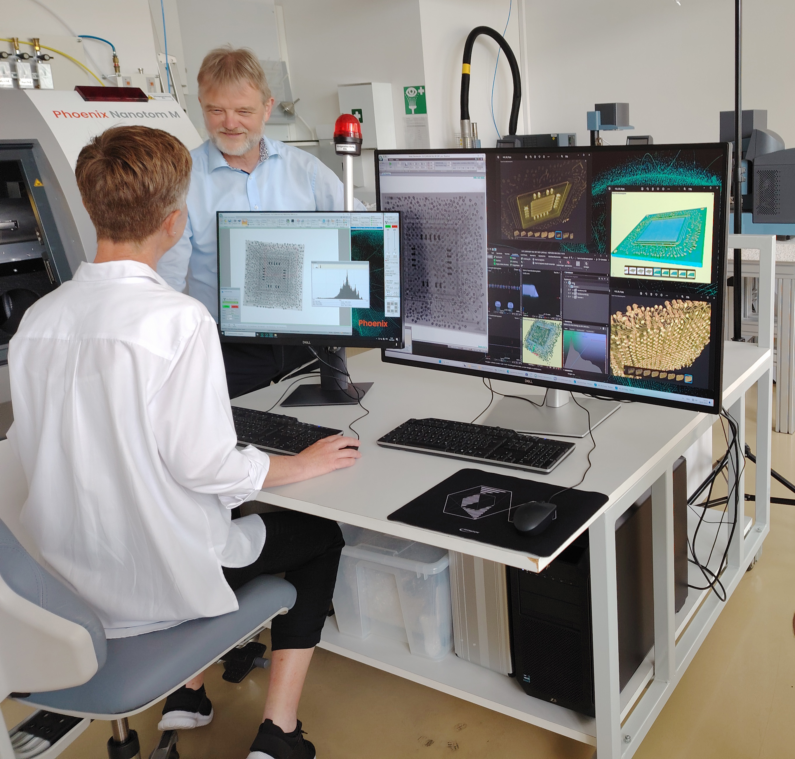
Microtechnology modules and systems have an extremely complex structure. When malfunctions and failures occur, the causes must be identified. We use X-ray computer tomograph (X-ray CT) for this purpose at Fraunhofer ENAS. This non-destructive analytical method enables the comprehensive inspection of electronic components and assemblies. This allows us to identify weak points and defects that are not distinguishable at first glance, especially from the outside.
The typical high-contrast “black and white” images of internal body structures are familiar from medical diagnostics. Are X-ray and CT images generated in the same way in science?
In medicine, radiological imaging is used to visualize injuries such as bone fractures. In this way, any symptoms that occur can be clearly assigned to diseases. We also use X-ray radiation in research to look inside components and assign symptomatic signs of failure to specific defects.
At Fraunhofer ENAS, we use X-ray CT to examine electronic and microelectronic assemblies and modules, as well as materials and composite materials, for weaknesses. This enables us to produce a high-resolution 3D volume image of the object – for example, of components from the automotive, aerospace, or electric mobility sectors. Unlike in human and veterinary medicine, where the patient is X-rayed in the CT system in their resting position and the signals are recorded by surrounding detectors, in industrial and scientific X-ray CTs, the component moves around its own axis in front of the X-ray tube.
The test specimen rotates 360° in the X-ray inspection system and is radiographed by the X-ray radiation. A volume data set is calculated from up to 3,000 automatically generated individual radiographic images. With software support, a high-resolution, three-dimensional and realistic image of the object to be examined is created from this data set. This 3D image reveals the internal structures of the component with a geometric magnification of up to 300 times and a high resolution of up to 0.3 micrometers.
Producing individual digital and detailed cross-sectional images from this volume image then enables us to view the inside of the component precisely, micrometer by micrometer – comparable to the typical “black and white” images used in medical CT diagnostics.
How can 3D and cross-sectional images be used to detect faults and defects in microtechnological components and assemblies?
By examining the component in all three spatial directions, it is possible to obtain a comprehensive picture of the object with all its internal characteristics and its condition. Possible and, above all, hidden defects can thus be detected and their geometry and exact position determined. This is proper detective work. For example, we can use this method to find out whether there are cracks in solder joints, whether bond wires are defective, or whether materials or material composites are faulty. We can also see in the images whether there are any air pockets or impurities that could cause defects in the long term.
If we know from the outset how defects manifest themselves, meaning that we know the specific symptoms, we can incorporate this information into our analysis and take a closer look at the typical weak points for these defects. For example, if there are indications that the power supply is interrupted, we know that the current-carrying paths require closer inspection. This narrows down the error and defect analysis.
Fraunhofer ENAS offers industrial users X-ray CTs as an investigation service for the condition and defect analysis of their assemblies and modules. What opportunities does this present for customers?
Fault and damage inspection is indispensable in the design and development process of new products. It can be used to identify weak points before the component is transferred to series production, and risks develop due to failures in the subsequent application. With our inspections, we support our customers on the way to a “zero-defect” strategy to ensure extremely high reliability through flawless electronic components at all times.
In subsequent thermo-mechanical stress tests, in which we expose the test specimens to extreme temperatures, humidity, vibrations, tension or pressure, we can also check whether an identified crack becomes critical under load – for example, whether it propagates or not.
In addition to analyzing defects, X-ray CT can also be used to draw conclusions about the suitability of new materials or material composites for technological innovations. If, for example, we detect abnormalities such as pores, delaminated areas or other deviating features in the composite, it may no longer be possible to guarantee the required characteristics of the composite material, which are, however, essential for the subsequent application.
Another special feature is that X-ray CT helps us to create numerical models for “digital twins” as exact virtual images of real, physical components. We can then simulate further developments and error corrections directly on the “digital twin” before new variants of the product are manufactured. For the customer, this digital process means enormous time and cost savings in the development of new products.
Thank you, Ms. Noack, for speaking to us and for giving us insight into the non-destructive inspection of electronic components.
Have we piqued your interest and would you like to benefit from our more than 15 years of expertise in the field of non-destructive inspection of electronic components, assemblies, modules or materials? Then please contact us.
Last modified: