 Fraunhofer Institute for Electronic Nano Systems
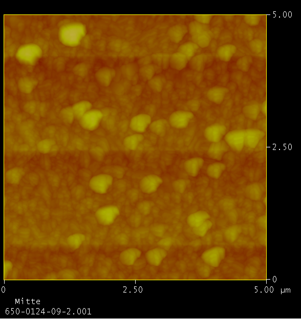
The surface modification before substrate bonding plays an important role. Regarding thick intermediate layers, such as glass frit or epoxy, the surface roughness of a wafer is insignificant for bonding. In contrast, when using bonding techniques without intermediates layers, surface roughness of wafers has a decisive influence to bring the wafer into atomic contact. For example, anodic bonding process requires a surface roughness less than 1nm. Other techniques use pretreatment processes such as plasma activation, hydrophilization or chemical mechanical polishing.
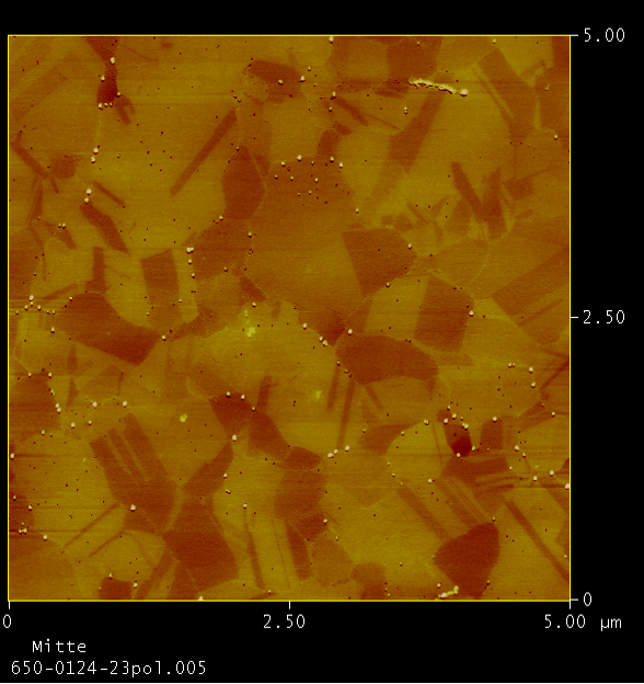
In addition to a wet-chemical pretreatment of the wafers, a chemical-reactive plasma discharge prior to bonding increases the mechanical strength of a direct-bonded stack. With these pretreatment (on local or the whole wafer area), the required annealing step can be dramatically reduced after pre-bonding procedure. The bonding strength is comparable to a high temperature direct bonding process and allows the joining of different heterogeneous materials with high CTE mismatch (e.g. lithium tantalate to silicon). The chemical mechanical polishing (CMP) has been developed and applied for the micro system technology or the 3D-Integration of different smart systems. Investigation objects are the extreme conditions of structure dimensions to structure distance as well as the variety of materials. The metal CMP e.g. aluminum, copper, gold, stainless steel or germanium for different 3D integration processes are just as important as the polishing of ceramics, glasses, silicon or silicon oxide. Application examples are novel SOI-substrates with buried silicide layers using in BiCMOS devices and high temperature applications.