Interview
Promoting young talent with prospects: Two trainees start their careers as microtechnology specialists at Fraunhofer ENAS and ZfM
Fraunhofer ENAS and the Center for Micro and Nano Technologies (ZfM) at Chemnitz University of Technology welcome two microtechnology trainees as new employees after the successful completion of their three-year training period. The two research and development partners are not only linked by a long-standing cooperation in many successful joint research projects. The Chemnitz institutions also work together closely in the training of junior scientists, thus creating optimal learning conditions for gaining practical experience.

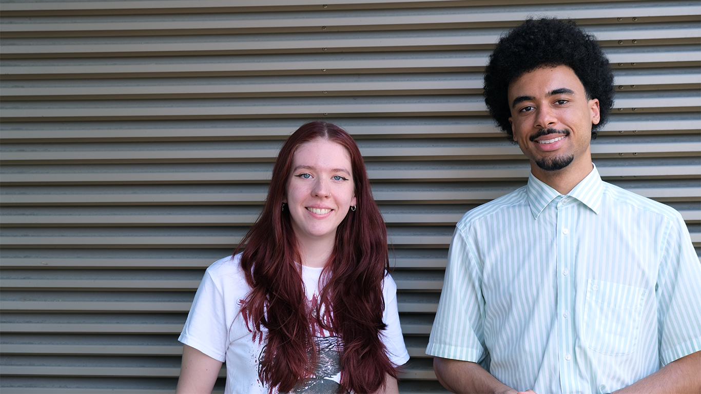
The trainees Lucie Hofmann and Kevin Müller were offered employment in August 2024 after passing their final exams. They are now an integral part of the expert teams in the field of gas phase deposition and scanning electron microscopy. In the interview, the two graduates talk about their time training at Fraunhofer ENAS, their work at the institute, special milestones and highlights they have experienced over the past three years, and their aspirations for their professional future.
First of all, congratulations on passing your exam. We look forward to working with you in the future. Lucie and Kevin, why did you decide to train at Fraunhofer ENAS almost three years ago?
Lucie Hofmann:
I previously studied electrical engineering and information technology at Chemnitz University of Technology because I have always been passionate about science and technology. However, I quickly realized that the degree course is very theoretical and that I would like an education with more practical relevance. I became aware of Fraunhofer ENAS through a tip from my friends and acquaintances. That’s how I found out about the opportunity to train as a microtechnologist and was immediately interested.
Kevin Müller:
I was also interested in science when choosing a career. Electrical engineering, chemistry, and physics have always been fields that I was passionate about and could imagine working in later. It was also important for me to find a training company in the Chemnitz region. Since Fraunhofer ENAS combines both, I was very pleased to be able to sign my training contract here.
What did you particularly like during your training at Fraunhofer ENAS?
Lucie Hofmann:
The core qualification seminar in Leipzig was a highlight for me. Together with trainees from other Fraunhofer Institutes, we were able to attend various courses there that taught us technical and social skills. For example, we took part in training on various presentation techniques and team-building activities. During this seminar, we not only learned more about the concept of the Fraunhofer-Gesellschaft as a research organization, but also had the opportunity to establish new contacts and gain insight into other Fraunhofer Institutes.
Kevin Müller:
That’s right, being able to exchange ideas with trainees from other Fraunhofer Institutes was definitely a highlight for me as well.
Another thing I particularly liked about the dual training format was that we were able to spend the second year of our training in the institute’s various research departments that process wafers. Thus, we got to know different areas of research at the institute and chose our focus or specialization corresponding to our personal interests in the third year of training.
Since we were able to gain a better understanding of the overall sequence of the various processes involved in wafer processing, getting to know the institute’s departments was also beneficial for vocational school. These processes included chemical and physical vapor deposition, in which various materials are applied to serve as conducting paths or insulators. We also gained experience in lithography, in which structural patterns are created in a light-sensitive photoresist, and in etching processes, which are used to transfer structures to the underlying layer. These processes were part of the theoretical curriculum as well. It was therefore helpful that we were able to experience the relevant departments and thus get to know the individual steps of wafer processing in practice.
Lucie Hofmann:
I agree with Kevin. We had a lot of freedom right from the start and were able to actively shape our training ourselves, decide what we were particularly interested in and develop in that direction. I don’t take that for granted.

You were able to choose a specific specialization during your training. Why did you, Kevin, choose scanning electron microscopy (SEM)?
Kevin Müller:
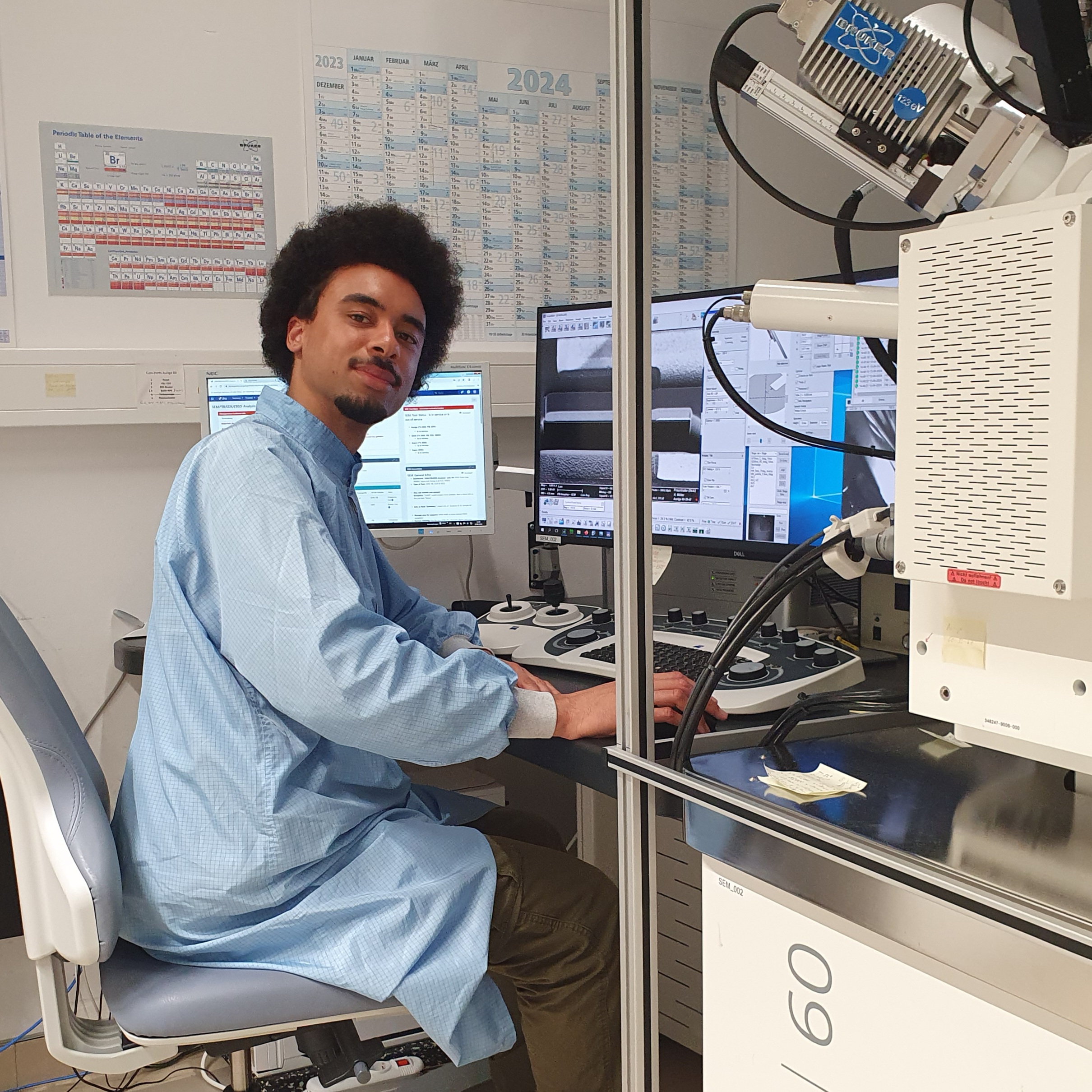
It was very exciting and amazing for me to see how even the smallest structures can be viewed in high resolution using SEM and how we can get so close to them. In the field of micro- and nanotechnologies, we generally cannot see directly what the structures we produce look like – neither with the naked eye nor with optical microscopy. But REM makes exactly that possible. For example, when layers are chemically removed from a wafer using etching processes and our colleagues want to examine this surface structuring, we can actually create a highly detailed image using SEM. This means that I am closely involved in the development of tiny microelectronic components at the smallest level. I was immediately captured by that.

And you, Lucie – why did you decide to specialize in the field of physical vapor deposition (PVD)?
Lucie Hofmann:
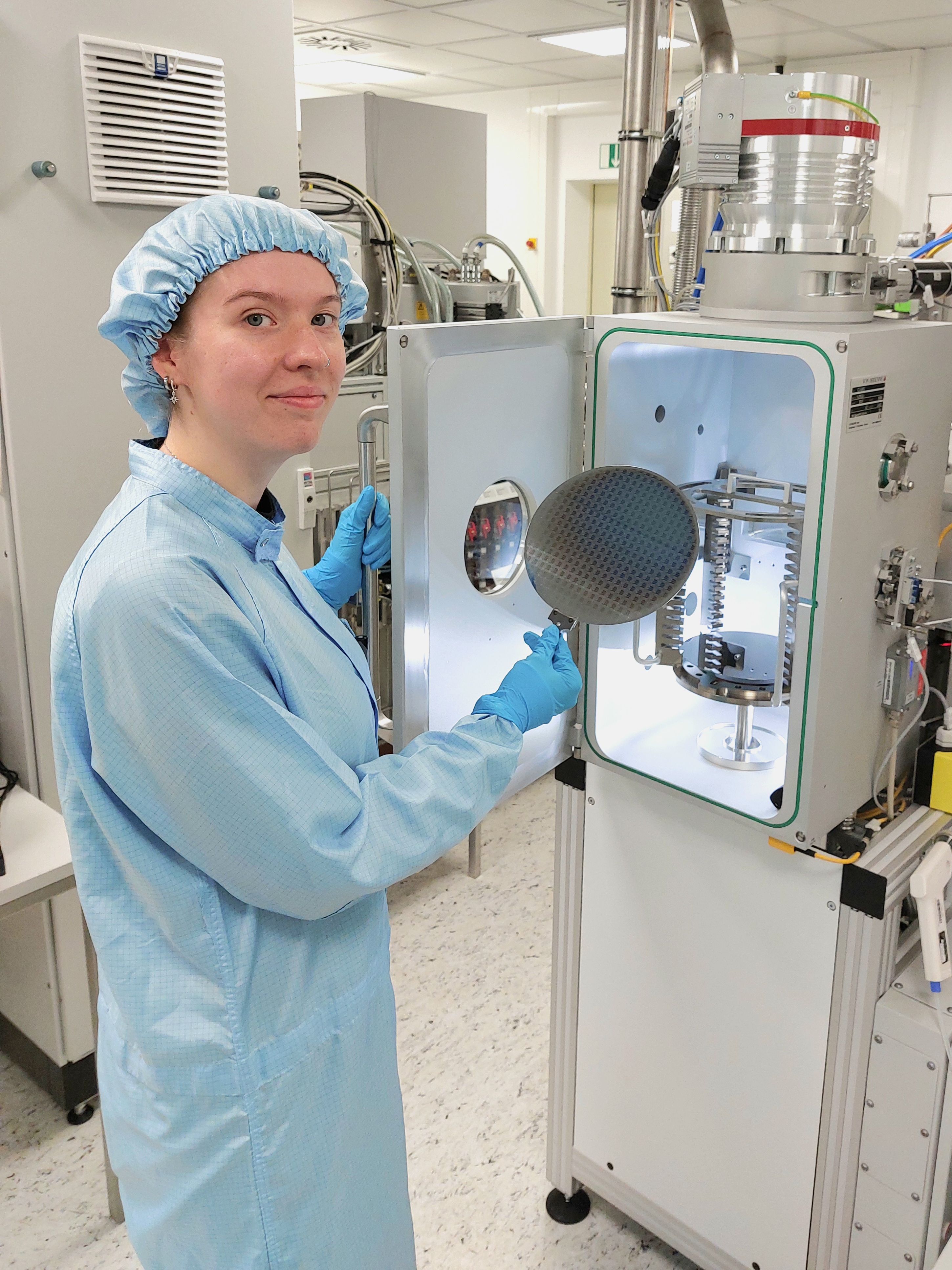
I was fascinated by the layer deposition systems and how they work right from the start.
With these systems, we can precisely deposit layers of copper, aluminum, or titanium, for example, in the micro- and nanometer range on various substrates such as silicon or glass.
I also got on particularly well with my colleagues in this department from the very beginning, so my decision to specialize in PVD was a relatively quick one.
What do you find particularly fascinating about your work?
Lucie Hofmann:
I think it’s great that I can support my colleagues with my work. The moments when other departments approach me and I can advise them on coating specific substrates so that they end up with the desired characteristics are just great.
Kevin Müller:
I feel the same way. It’s pretty cool when colleagues want to examine the composition of a sample, I can help them, and we obtain a satisfactory result together. I really enjoy contributing to research success with my specialist knowledge.
You were kept on after successfully completing your final exam and will play an important role in the development of smart systems in future. What are you most looking forward to now?
Kevin Müller:
I plan to take training in another SEM analytical method, known as energy-dispersive X-ray spectroscopy, in the near future, so that I can analyze and evaluate samples even more precisely. In general, I just want to familiarize myself even better with the technologies I work with and continue to learn a lot from my colleagues.
Lucie Hofmann:
It’s similar for me. I want to settle into my day-to-day work and am looking forward to keep learning as much as possible from my colleagues.
If you had one wish for your future at Fraunhofer ENAS and the ZfM, what would it be?
Lucie Hofmann:
I hope there will always be lots of exciting research projects for me to work on. It is always fascinating to see what is possible in the field of micro- and nanotechnology and I hope to be involved in many more projects in the future.
Kevin Müller:
My wish for the future? I hope that I can acquire even more knowledge and skills in the coming months and years, so that I can do this job better and better.
In short, I would like things to continue just as they are.
Thank you, Lucie and Kevin, for this interview and for sharing your insights and experiences.
As a research institute, Fraunhofer ENAS offers a modern, international working environment, as well as diverse tasks with creative freedom and responsibility in the scientific, technical and administrative fields.
The institute has been training microtechnologists since 2009 and is actively involved in promoting young talent in Chemnitz and the region.
For further information on current job vacancies and training opportunities at Fraunhofer ENAS, visit the career pages.
Last modified:
 Fraunhofer Institute for Electronic Nano Systems