 Fraunhofer Institute for Electronic Nano Systems
Cleaning
| RCA clean |
| DI-water flushing |

© Jürgen Lösel for cfaed, TU Chemnitz
© Fraunhofer ENAS
© Fraunhofer ENAS
© Fraunhofer ENAS
© Fraunhofer ENAS
| RCA clean |
| DI-water flushing |
| Thermal oxidation | Dry, wet, HCl |
| Annealing | Inert, reducing, oxidizing, ambient and forming gas |
| Sputtering | Metallization | Ag, Al, Au, Co, Cr, Cu, Mo, Ni, Pd, Pt, Ru, Sc, Ta, Ti, W, Nb, Zr |
| Metal alloys | AlSiCu, AlSi, AlTi, AlGe, TiPd, CrPd | |
| Metallic glass | PdCuSi, AlTiW, CuCrPd, (AlNiY), (NiNbZr) | |
| Memristive | BiFeO3, TiO2, TixO(2x-1) | |
| Oxides, Nitrides | Al2O3, CuOx, SiO2, TaN, Ta2O5, TiN, TiO2, Pyrex | |
| Piezoelectric | AlN, AlScN | |
| Photonics, Optics | AlN, ITO | |
| Semiconductors | Ge, Si | |
| Spintronics | Ni, NiFeCr, Ru, Pt, Cu, Al, Co, MgO, MnIr20, Co40Fe40B20, Ni81Fe19, Co90Fe10, Co20Fe60B20 | |
| Superconductors | CeO2, SrTiO3, YBa2Cu3O7 | |
| Packaging | Al-Pd-Multilayer, Ti-Si-Multilayer, CuO-Al-Multilayer | |
| Phase Change | GeTe, Ge2Sb2Te5 | |
| Ion beam sputter deposition (IBSD) | Al, Co, Cr, Cu, Mo, Ni, Ru, Ta, Pt, Ti, Y, Sc | |
| Electron beam evaporation | Al, Co, Cu, Ni, Pd, Pt | |
| Thermal evaporation (follow up processes under inert atmosphere possible) | ||
| Organic semiconductors | ||
| Metal oxides (e.g., MoO3) | ||
| Metals (e.g., Ca) | ||
| Dielectrics (e.g., LiF) | ||
| Plasma enhanced CVD | TEOS-SiO2, SiO2, Si3N4, SixOyNz, SiCOH, CF/CH polymers, amorphous silicon, diamond-like carbon, CNTs |
| Low-Pressure CVD | Si3N4, polysilicon, SWCNT/MWCNT |
| Metal-organic CVD | Cu, Co, TiN |
| CVD | Parylene N, C, D, F, AF4 |
| Metals | Co |
| Metal oxides | Al2O3, TiO2, HfO2, ZnO |
| Electrochemical deposition (ECD) | Au, Cu, Ni, Pd, Sn, SnAg, Al (ionic liquids) | |
| In development | In, Ga | |
| Nanomaterial dispersion preparation and analytics | |
| Dispersion-based assembly of semiconducting CNTs on waferlevel | |
| CVD of vertically-aligned CNTs (VACNT) | |
| Printing on multilayer graphene | |
| Transfer of monolayer graphene | |
| Transfer of VACNTs | |
| Nano device integration steps: structuring, cleaning, contacting, functionalization, passivation | |
| Spin coating under inert atmosphere | |
| Nanoparticle dispersions (e.g., ZnO, quantum dots) | |
| Organic semiconductors | |
| Polymers | |
| Electron beam lithography | Resolution: < 50 nm |
| Projection lithography | 350 nm |
| Contact lithography | 2 µm |
| Nano imprint lithography | Resolution: 50 nm |
| Grayscale lithography with electron beam lithography and projection lithography | |
| Double side lithography | |
| Mix and match lithography (electron beam lithography and projection lithography in one resist layer or in sequential resist layers) | |
| Spray coating (thin to thick resists) | |
| Positive tone resist: 3.6 - 14.5 µm (different resists) | |
| Negative tone resist: 5.5 - 11 µm (different resists) | |
| Spin coating (thin to thick resists) | |
| Positive tone resist: from 0.2 - 100 µm (different resists) | |
| Negative tone resist: from 0.2 - 100 µm (different resists) | |
| CD-SEM characterization | |
| Confocal microscope characterization | |
| Thin and thick wafer substrates of different material and wafer size | |
| NIL mastering | |
| Plasma strip | Oxidizing, reducing |
| Wet processes | ||
| Metals | Al, Au, Cr, Cu, Pt, Ti, W, Ag, Pd, Sn | |
| Non-metals | AlN, CuxO, Si3N4, SiO2, Si, polysilicon, glass, ITO, ZnO, BFO, HfO2 | |
| Dry processes | ||
| Metals | Al, Cr, Cu, Ti, Ta, TiW, W | |
| Non-metals | Si, polysilicon, SiC, SiO2, Si3N4, silicides, TiN, resists, glass, low-k dielectrics | |
| Deep reactive ion etching | Si | |
| Lift-off | ||
| Gas phase etching of SiO2 | ||
| Assembly of CNTs | ||
| CMP for patterning | Al, Cu, Ge, Si, SiO2, W, barriers (TiN/Ti, TaN/Ta), ceramics (LiNbO3, LiTaO3), glass, isolators, stainless steel | |
| Planarization and surface finishing | ||
| Grinding | Si, glass, ceramics | |
| Spin etch | Si, glass | |
| Through Silicon Vias (TSVs) | ||||
| Integration concepts | via last, via middle | |||
| TSV type | full fill, conformal metallization | |||
| Substrates | silicon, glass | |||
| Main processes | deep etch, isolation, box-etch, metallization | |||
| Post-TSV process | Front-/backside RDL incl. UBM | |||
| Wafer thinning | Si, glass, ceramics | |||
| Thin wafer handling | Temporary bond, Taiko wafer | |||
| Wafer bonding | Hybrid, thermocompression, fusion, etc. | |||
| Biocompatible packaging (Parylene (C, D, F)) incl. pre-treatment (silanization) | ||
| High aspect ratio microstructures |
| Conventional, permanent wafer bonding | ||
| Silicon fusion bonding and plasma-activated bonding | RT - 100 °C, 100 °C - 200 °C, 200 °C - 400 °C, > 400 °C / Si, borosilicate glass, foturan glass, quartz glass, LiTaO3, LTCC, stainless steel | |
| Anodic bonding | RT - 550 °C, 0 - 500 kPa, 0 - 2.000 V, Si, SiO2, Si3N4, borofloat, pyrex, SD2 |
|
| Glass frit bonding (leaded and lead-free) | Si, glass | |
| Eutectic bonding | Au-Si, Au-Sn, Al-Ge | |
| Thermo compression bonding | Al-Al, Cu-Cu, Au-Au (nanoporous gold), plasma enhanced Cu-Cu bonding | |
| SLID bonding | Au-In, Au-Sn, Cu-In, Cu-Sn | |
| Low-temperature, permanent wafer bonding | ||
| Reactive bonding | Si, Al2O3, Al, Cu, borosilicate glass, foturan glass, quartz glass, LiTaO3, covar, stainless steel | |
| Plasma activated bonding | glass-frit, glass-silicon | |
| Hybrid bonding | SiO2/Cu | |
| Sintering | Ag, Cu | |
| Characterization and analysis | ||
| Yield, bond strength, hermeticity, SAM, interface material analysis, cross-section, SEM, FIB | ||
| Temporary wafer bonding | ||
| Bonding and debonding | thin wafer processing | |
| Wire bonding | ||
| Al-Si | 18, 32 µm | |
| Al | 125, 250, 300 µm | |
| Au | 25, 30, 50, 125 µm | |
| Cu | 32 µm | |
| Chip bonding | Flip-chip, chip-to-chip (C2C), chip-to-wafer (C2W), multi-chip-module (MCM), chip-to-board (C2B), surface-mounting technology (SMT), printed contacts | |
| Encasings and Caps | Metal, glass, ceramics, plastics, thin film encapsulation (Parylene) | |
| Dicing | 4" to 8" | Silicon, glass, metals, compound materials |
| Picosecond laser (10 W) | 266 nm, 355 nm, 532 nm, 1064 nm, pulsed energy | |
| Thulium fiber laser (20 W) | 1908 nm, continuous wave | |
| Key facts | Feature size down to 10 µm | |
| Positioning accuracy 0.5 µm | ||
| Camer-based alignment | ||
| Materials | ||
| Polymers |
PC, PMMA, PET, COC, acrylic resin, adhesive tapes (incl. cover sheets) |
|
| Ceramics | LiTaO3, Al2O3, LiNbO3, PZT | |
| Metals | Al, Mo, Au, Pd, stainless steel | |
| Glass | borofloat, quartz, BK7, microscope slides | |
| Semiconductors | Si (mono and polycrystalline), ITO | |
| Others | solder, reactive foils, films with nanoparticles | |
| Processes | ||
| Cutting, drilling, 2.5D structuring, marking, trimming | ||
| Polymer welding | ||
| Customer-specific process development | ||
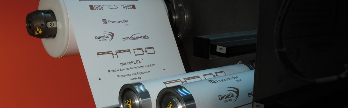
| Inkjet | Sheet-fed, web-fed (R2R), robot-guided on 3D objects | |
| Aerosol jet | Sheet-fed | |
| Dispensing | Robot-guided on 3D objects | |
| Screen | Sheet-fed, web-fed (R2R) | |
| Functionality formation by sintering | Thermal, IR, UV, electrical, chemical, plasma, laser, IPL, excimer lamp | |
| Materials | ||
| Inks | Conductive inks: Ag, Cu, Au, C, Zn, ..., semiconductive inks (organic and oxide-based), dielectric inks (organic) | |
| Substrates | Polymer films (PET, PEN, PI, PC, PVC, PP, ...), paper (uncoated and coated), congurated cardboard, glass, ceramics, textiles, sheet metal, rubber | |
For your support, we offer the following research and development services: