 Fraunhofer Institute for Electronic Nano Systems
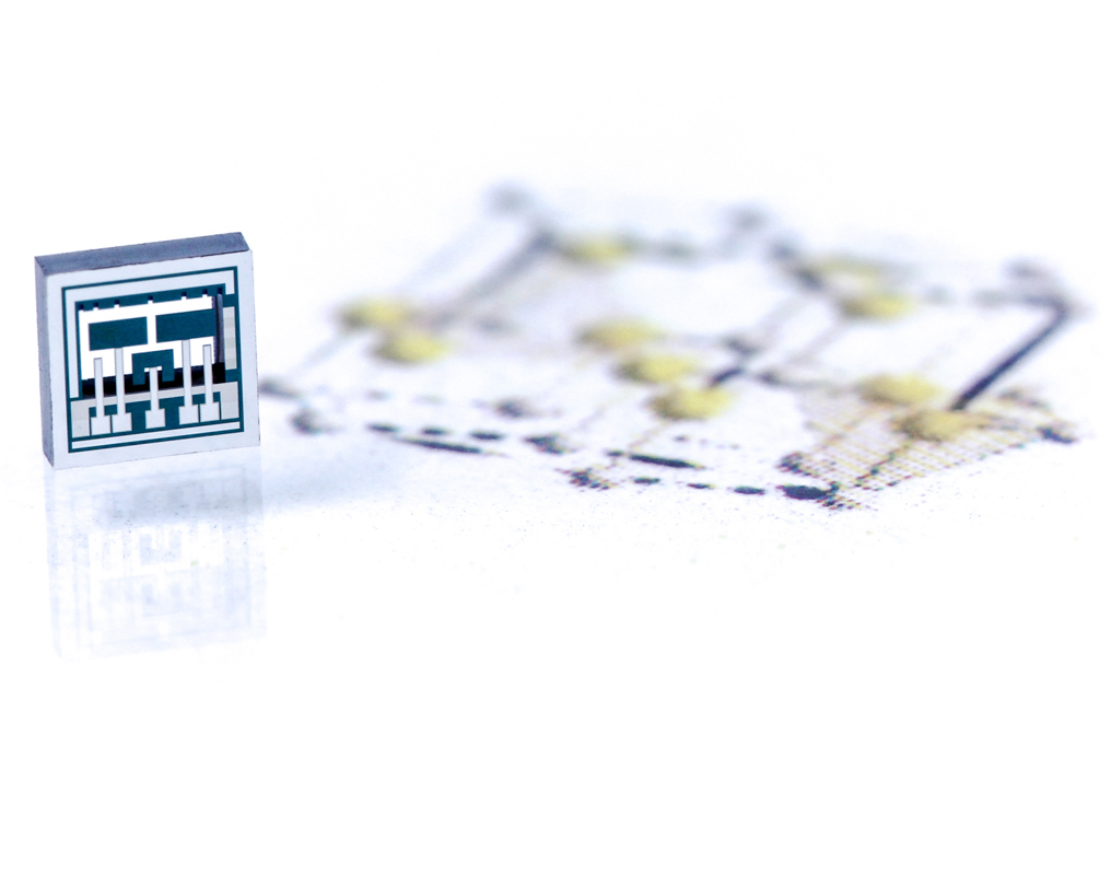
This technology platform is based on the utilization of piezoelectric aluminum nitride (AlN) for the actuation of moving structures or for the detection of very small movements. A sputtering process was developed and optimized for the deposition of piezoelectric AlN. The deposition takes place directly on (111)-Si or on a special electrode material. Another electrode is structured above the AlN and enables the electrical control of the elements. In contrast to conventionally used lead-zirconium titanate (PZT), this technology is C-MOS compatible, as deposition and structuring can be realized with conventional systems for aluminum-based BEOL technologies.
The process sequence for the production of the AlN thin-film system can be integrated into various technology sequences for Si or SOI wafers and combined with the production of spring-mass systems, tongue elements or membranes.
The technology platform is established on a 6" wafer size and is constantly being further developed. An expansion to 8" wafer size and the integration of AlScN are the subject of current development projects.
Already realized application examples are micromechanical mirrors e.g. for use in an endoscope or wake-up generators for energy-self-sufficient and current less detection of mechanical events (such as acceleration or vibration).
Further application possibilities under investigation are membrane-based MEMS such as pressure sensors or ultrasonic transducers as well as viscosity sensors that can be operated in both gases and liquids.