 Fraunhofer Institute for Electronic Nano Systems
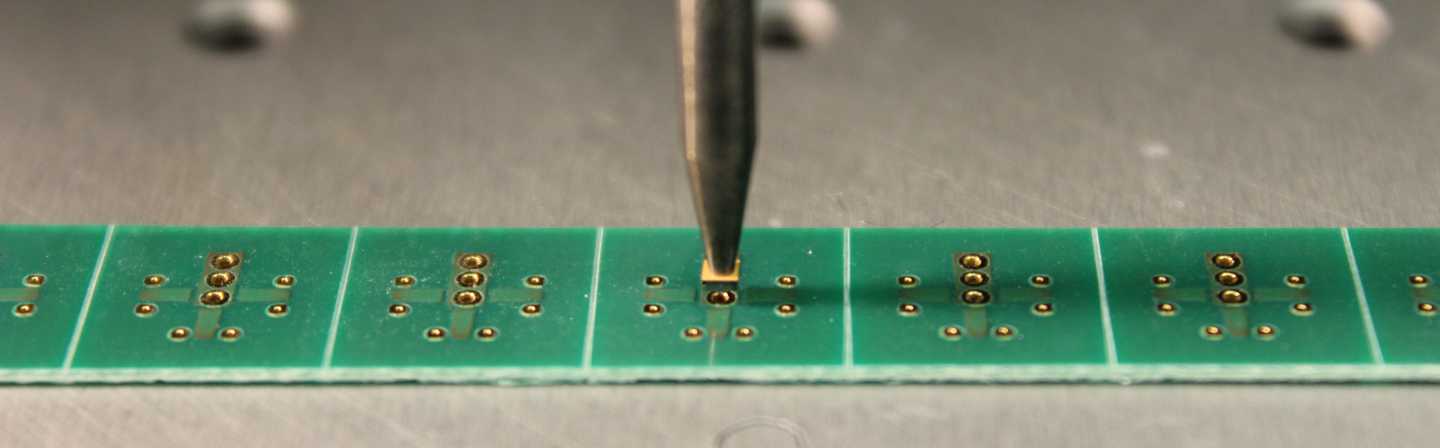
Chip bonding as a first level packaging technologie is mainly used for the bonding of fabricated and separated chips onto different types of substrates. Mainly used bonding technologies are eutectic bonding as well as adhesive bonding. Intermediate bonding layers are epoxies, ceramic adhesive media, pastes or solder (SnAg, SnAu, SnCu) which can be deposited. Most of these packaging technologies are used in sensors, actuators or microsystems which can be applied for manufacturing of prototypes and small series. A Tresky T-3002-M chip bonder (Dr. Tresky AG, Switzerland) is available in our laboratories. This tool allows a precise x-y-positioning and thus an accurate alignment of chips onto substrates of up to 8" size can be ensured.
Bonding technologies
- Flip-Chip (FC)
- Chip-to-Chip (C2C)
- Chip-to-Wafer (C2W)
- Multi-Chip-Module (MCM)
- Chip-on-Board (COB)
- Surface Mounted Devices (SMD)
Substrates
- Lead frames
- Silicon wafers
- Ceramics
- Printed circuit boards (PCB)
- Electronic packages