

The properties of nanomaterials such as CNTs or graphene can give significant improvements in many sensoric and electronic applications. To achieve an industrial implementation various technological challenges must be addressed guided by nanomaterial compatible integration technologies, real performance, and cost.
In-plane semiconducting and metallic nanolayers
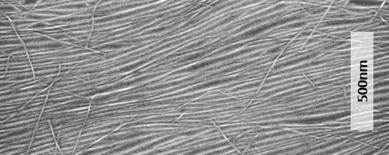
At Fraunhofer ENAS a technological platform was created giving solutions for the integration of CNTs and graphene in the environment of wafer-level microtechnologies. We can provide wafer processes for semiconducting CNT layers in a quality used in short channel FETs with a high yield. For high-performance functionalities, we develop scalable processes enabling even a high level of order in semiconducting films composed of highly dense and parallel aligned CNTs. The strength of this technology lies on the one hand in a substrate-free semiconductor technology enabling various 3D integration concepts. On the other side, this technology enables unique advantages in high-performance applications such as analog high-frequency communication electronics, THz polarizers or environmental sensors with a significantly enhanced sensitivity.
Vertically assembled nanostructures
For any applications benefiting of high surface area nanostructures such as electrodes, Fraunhofer ENAS provides integration service for CVD-grown CNTs on customized substrates. This covers patterned growth of single-walled or multi-walled CNTs on wiring systems at growth temperatures reaching down to 450°C. Several integration scenarios have been demonstrated for MOEMS with integrated heatable CNTs on SiN membranes, vertical interconnects for advanced BEOL in ULSI, flexible flip chip interconnects, sensing networks for e.g. tactile forces as well as gas adsorbers. Along with this, we provide also special solutions for the integration of pristine CNT forests at room temperature combined with the unique advantage of configurable contact interfaces and substrates. For example, we have achieved a rather simple process for a nanomembrane-like electrode system composed of a few µm thick parylene substrate, a free configurable in-plane conductive layer, and a vertical CNT forest with >10 µm. In the current state, the process allows fast fabrication of 200 mm-sized nanostructured foils. This configuration was successfully tested in a flexible supercap device and opens many more possibilities in flexible electronics.
 Fraunhofer Institute for Electronic Nano Systems