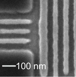
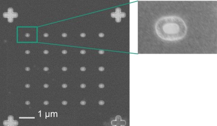
The production and integration of highly precise nanodimensional pathways or waveguides is relevant for all technologies involved in the manufacturing and scaling of quantum chips. This precision is crucial for controlling quantum bits (qubits), as well as for scaling components and integrating the various components of the quantum chip to create complex structures with high density and functionality.
At Fraunhofer ENAS, we utilize established semiconductor technology manufacturing techniques to process various substrates and materials at the nanotechnological level. In-house developed processes, such as the Intra-Level Mix & Match approach (ILM&M), are used to structure the same resist layer using electron beam lithography and i-line stepper lithography. This allows for significantly reduced writing times while simultaneously taking advantage of the equipment's resolution (< 350 nm E-Beam, > 350 nm i-line) in combination with high flexibility and throughput.
These advances in nanotechnology enable the development of quantum computers by allowing new materials, manufacturing techniques, and designs that improve the performance and scalability of quantum computers.
 Fraunhofer Institute for Electronic Nano Systems
