 Fraunhofer Institute for Electronic Nano Systems
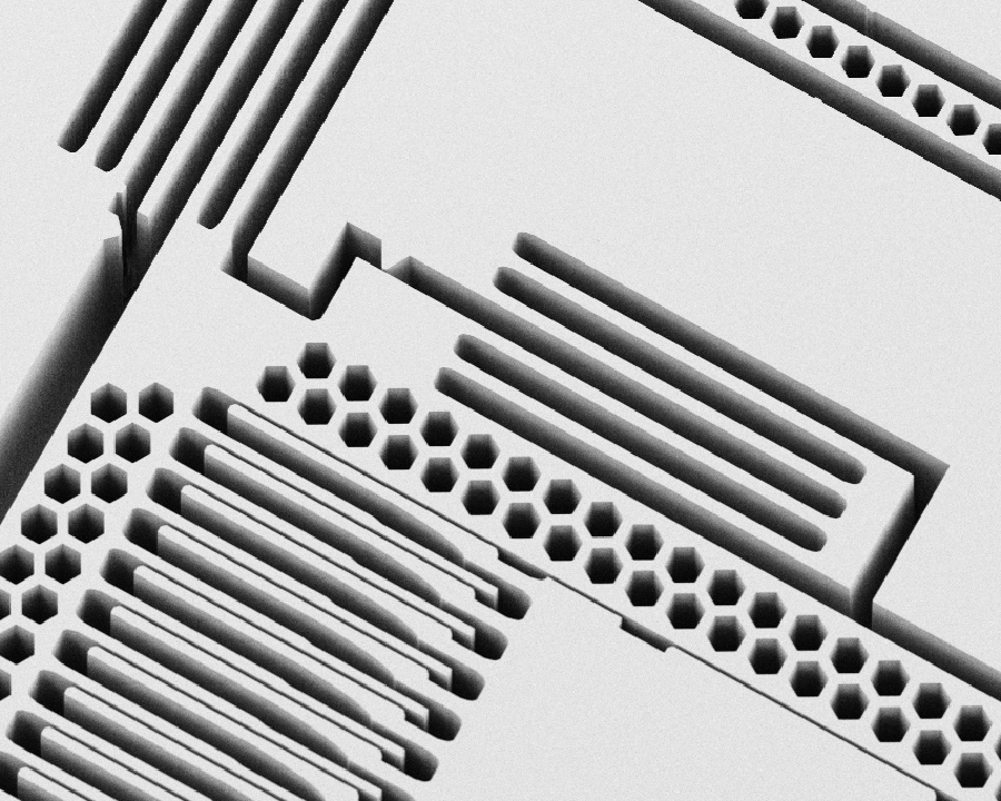
This technology platform based on wafer compounds with pre-structured cavity enables in particular the fabrication of electrostatic actuators and capacitive sensors with high aspect ratios (AR up to 40) for the precise detection of very small movements in up to 3 dimensions. This concept provides many degrees of freedom in the designs.
The patented technology variant BDRIE-HS* (High Sensitivity) enables the etching of vertical trenches down to the sub-μm range in combination with areas with large structural heights to achieve large masses, e.g. for low-noise inertial sensors.
The technology platform can be used in a glass-silicon variant as well as in a full-silicon variant. In combination with various integration concepts and encapsulation technologies at wafer level, internal and external rewiring as well as vertical vias are possible to achieve a compact design.
By hermetic encapsulation based on wafer bonding methods, the internal pressure within the sensors can be adapted to the requirements of the applications in a wide range. The optional use of getter material enables residual gas pressures down to the μbar range to achieve high mechanical quality factors.
The technology platform is currently established with verified design rules on 6" wafer size and is constantly being further developed. Application examples are e.g. MEMS inertial sensors for measuring accelerations, vibrations and angular velocities (rotation rates) as well as spring force normals and measuring tips.