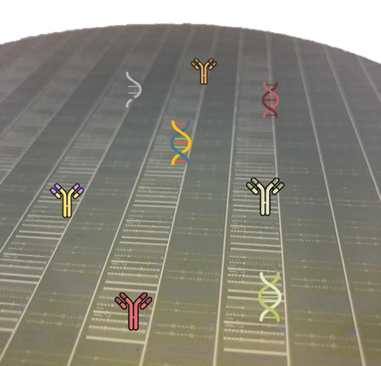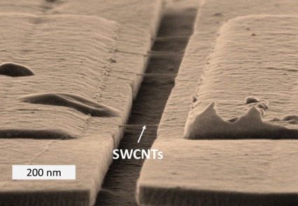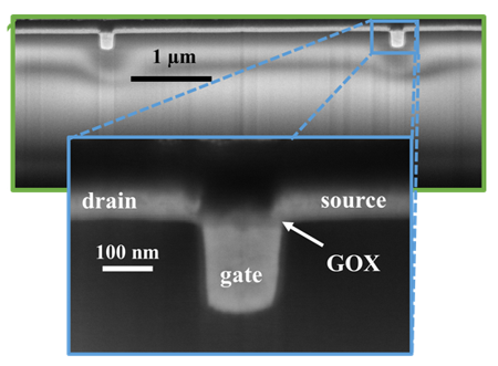


Giving rise to outstanding properties of 1D and 2D nanomaterials, Fraunhofer ENAS develops scalable wafer-level device technologies considering the process chain starting from source material until heterogeneous integration culminating in monolithic on-top-of-CMOS integration scenarios.
In the cooperation between ENAS and ZfM a versatile CNT-based FET platform was developed. Our R&D focus lies on reliable wafer-level device manufacturing and high compatibility with conventional microtechnologies.
Carbon Nanotube-based Field-Effect Transistors for electronics
Carbon nanotubes (CNT) are one of the few nanomaterials surpassing incumbent bulk semiconductors like silicon in terms of intrinsic properties such as charge carrier mobility but also in integration capabilities not constraint by substrates. Thus, thin semiconducting films as e.g. thin film transistors (TFTs) can add functionalities to conventional IC architectures or to alternative technology routes for flexible electronics. At Fraunhofer ENAS we provide a technology module for CNT-FETs on 200 mm diameter substrates. We develop high-yield processes for short channel FETs, application specific functionalization as well as integration into heterogeneous systems. We can provide hardware solutions for various sensoric tasks in bio-sensing, gas sensing, reaching to quantum sensing. Moreover building blocks in electronics can be addressed such as hardware security elements or high frequency nanodevices. To emphasize, most recent research demonstrate analog high frequency (HF) CNT-based field-effect transistors (CNTFETs) featuring higher transit frequencies compared to silicon HF FETs for a similar technology node. For industrial implementation of this new technology the Fraunhofer ENAS conducts research on device technologies for HF circuits with highly linear amplifiers arising from the unique 1D material configuration.
Nanodevices for bio sensing
On the basis of the CNT FET technology module at Fraunhofer ENAS, we foster the development of cheap, fast, and sensitive methods for monitoring analytes required in many areas such as drug discovery, real-time detection of biomarkers, air, and water monitoring, food industry regulation, and on the control of rapidly spreading diseases. Biosensors are platforms that can detect biological and chemical species when combined with a biorecognition element and a transducer for signal decoding and, ideally, such platforms are highly specific and provide high sensitivity on pbm-level for the target of interest. Field-effect-based biosensors (Bio-FET) offers the advantages of direct and label-free measurements, resulting in a faster read-out of results, besides the possibility of miniaturization and large-scale fabrication. In addition, Bio-FET platforms can be easily functionalized, where an on-demand immobilization of antigens, oligonucleotides, aptamers, proteins, enzymes or even whole cells can be realized upon request.
Stressconfigurable Nanodevices
Strain in nanostructures is of fundamental importance for device functionality and reliable device manufacturing. Control of strain in 1D and 2D nanomaterials promotes suspended sensor configuration with unique sensitivities. Strain will be essential for NEMS devices to operate at certain frequencies and is even a prerequisite for sensitive strain sensors operating at low strain states. Finally, it is important to consider in integration technologies since most of deposition techniques for e.g. graphene are effected by undefined strain states such as wrinkles causing unreliable device properties.
At Fraunhofer ENAS in cooperation with the Center for Microtechnologies (Chemnitz University of Technology), we perform R&D on strain configurable nanodevices. A surface technology was established which allows unique control of strain states defined by design. Hence, device arrays with extremely small footprint and broad-band tuned bandgaps become possible. The technology was already successfully demonstrated on-top of CMOS at 200 mm wafer level.
 Fraunhofer Institute for Electronic Nano Systems