 Fraunhofer Institute for Electronic Nano Systems
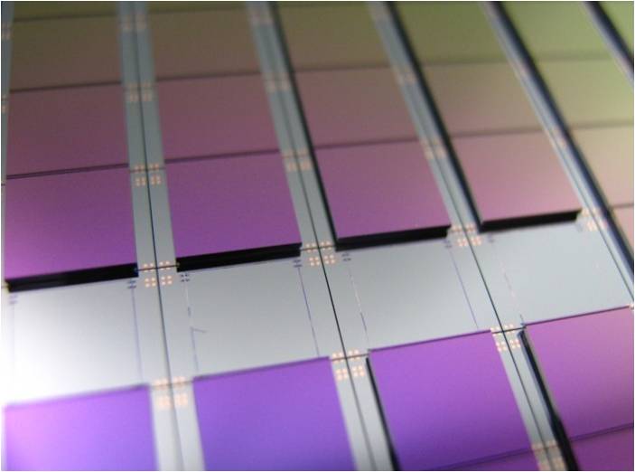
For the system integration, various concepts like System-on-Chip (SoC), System-in-Package (SiP) or System-on-Package (SoP), have been developed. Novel SiP concepts introduce the third dimension, which results in complex system architectures. The 3D integration by Through Silicon Vias (TSV) or Through Glas Vias (TGV) is one of the most promising approaches. However, 3D integration by TSV or TGV is challenging due to numerous and customized types of MEMS manufacturing processes, material combinations and packaging methods. In addition, requirements regarding the ambiance and its media have to be fulfilled, such as openings for pressure equalization for pressure sensors or a hermetic sealing for acceleration sensors. Therefore, the advanced 3D integration techniques known from microelectronics cannot easily be transferred to MEMS. Instead, different constraints demand different approaches for the integration of MEMS.
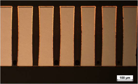
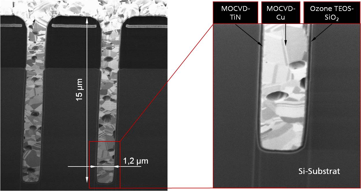
In general, the 3D integration process is divided in four steps:
- Forming of the vias with deep structures and isolation
- Metallization of the vias
- Wafer thinning and planarization
- Permanent and temporary wafer bonding
These four steps can be combined in different order with different resulting process operations.