 Fraunhofer Institute for Electronic Nano Systems
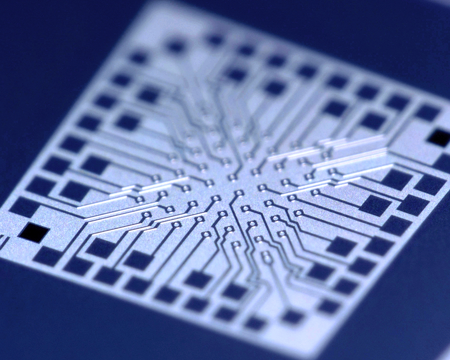
This technology platform enables the structuring of thin membranes based on silicon wafers or SOI wafers, also using wafer bonding processes. The membranes can consist of different thin layers or layer stacks. Established material systems include e.g. the membrane materials Si, SiO2, Si3N4, AlN, and graphene as well as electrode materials such as Al, Au, Pt and Metallic glass?
After assembly, the membranes are exposed by thinning and etching processes using selective etching technology.
The technology platform is established on 6" wafer size and is under continuous development. Current examples of devices are CMUT and PMUT for applications in non-destructive monitoring/analysis of materials, distance measurement, object detection, liquid level measurement and endoscopic and acoustic and photoacoustic imaging. Further applications of these technologies are e.g. pressure sensors as well as optical filters and shutters.