 Fraunhofer Institute for Electronic Nano Systems
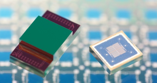
The focus of the applied research of department System Packaging are technologies both for the packaging of MEMS and NEMS in different packaging levels as well as for micro- and nanostructuring of surfaces in microsystems technology. In addition to the standard wafer bonding methods such as silicon direct bonding, anodic, eutectic, adhesive and glass frit bonding also more novel wafer bonding methods such as laser assisted bonding, reactive bonding as well as low temperature and thermo-compression bonding are investigated and developed for specific fields of application. All wafer bonding techniques are characterized in terms of bonding quality, strength and hermiticity to ensure their suitability for certain applications.
The department’s competence includes dicing, chip- and wire bonding as well as technologies for the integration of complex, miniaturized and intelligent systems. The integration possibilities are various ranging from hybrid integration of components on application-specific substrates, through the monolithic integration of electronic, sensoric and actuatoric components on silicon substrates (interposer), to the vertical integration of stacking components into the 3rd dimension on chip and wafer level (3D integration). Besides functionality and reliability, both miniaturization and integration represent the major challenges for the technology trend „More-than-Moore“. The department System Packaging contributes significantly to the implementation of this trend into new, custom applications.