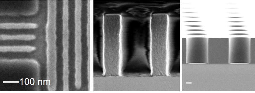
At Fraunhofer ENAS, various exposure processes are available in lithography. Depending on the method, the following structure sizes can be achieved:
- UV contact and proximity exposure (1:1) up to 2 µm
- UV projection exposure (stepper) up to 400 nm
- Electron beam exposure up to 40 nm for industry-relevant applications
Nanostructures below 40 nm are also feasible for feasibility studies as well as research and development work using electron beam exposure. Furthermore, the use of Nano-Imprint Lithography (NIL) for nanoscale structure sizes can also realize cost-effective production for a larger number of wafers.
Mix and match exposures of electron beam and UV projection exposure also provide an efficient way to realize nanostructures with efficient exposure times.
In addition to various materials and substrates, 150 mm and 200 mm substrates (Si, glass, etc.) can be flexibly processed in the fully automatic tools at Fraunhofer ENAS. 100 mm and special substrates (not SEMI-standard, significantly thicker substrates up to "chips") can also be processed using suitable adapter wafer or chucking solutions.
For resist coating, Fraunhofer ENAS offers not only low-viscosity high-resolution resists with layer thicknesses in the nanometer range but also high-viscosity and thus very thick resists up to > 100 µm layer thickness, as well as spray coating, especially for the realization of MEMS applications. Specifically, this allows lithography of, for example, wafers with cavities or perforations for a variety of MEMS applications. Double-sided lithography (front and backside) is also possible.
 Fraunhofer Institute for Electronic Nano Systems