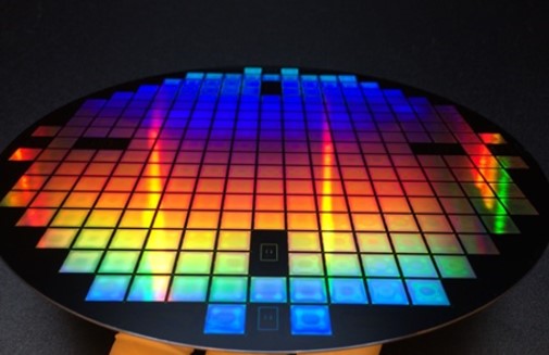
The plasma-based structuring at Fraunhofer ENAS relies on the availability of 11 machines used for both research and process development as well as production at the institute. Established structuring methods for materials like silicon, silicon dioxide, or aluminum, commonly used in microelectronics, are applied, especially for serving MEMS/NEMS and integration technologies. The portfolio also includes processes for structuring materials such as chromium, titanium, tungsten, or tantalum using molecular reactive plasmas. Both chlorine-based and fluorine-based plasmas at Fraunhofer ENAS are consistently customized to meet the specific requirements of the customer and the substrate being structured. The institute focuses on structuring materials essential for LED technology, such as gallium arsenide and gallium nitride, and methane-based structure transfer in indium tin oxide. Increasingly, these optical components require the transfer of spherical or otherwise defined geometries. Solutions for 2.5-D structuring have already been realized at the institute through various approaches (e.g., in combination with grayscale lithography). For the continuously growing fields of quantum sensing, neuromorphic systems, and quantum technology, ion beam etching processes are becoming increasingly important. For instance, certain spintronic applications require the layer removal of multilayer stacks whose chemical components do not form volatile etching products, which is why ion beam etching processes are also being investigated and developed at Fraunhofer ENAS.
 Fraunhofer Institute for Electronic Nano Systems