 Fraunhofer Institute for Electronic Nano Systems
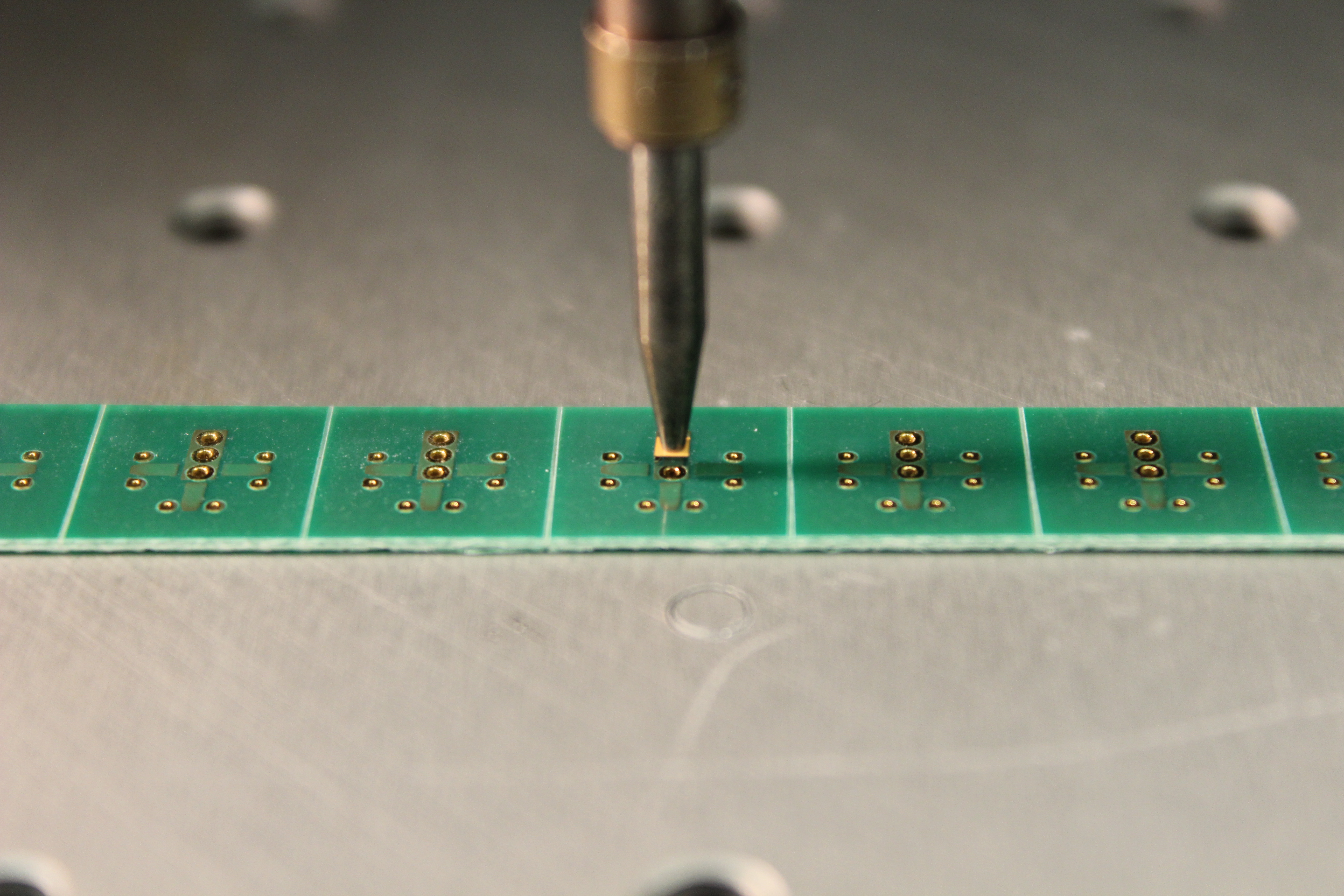
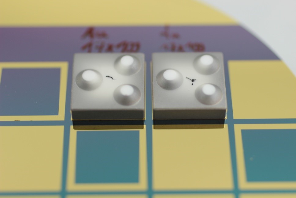
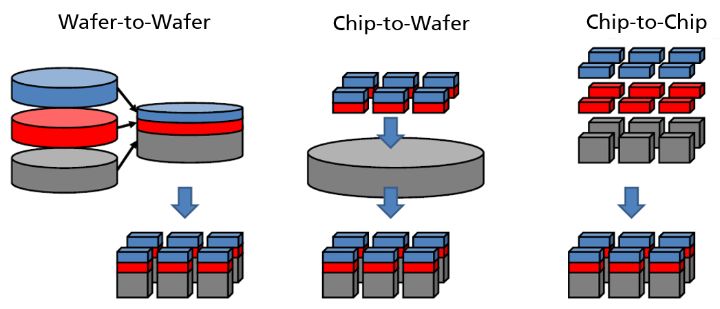
Usually, functional blocks are integrated two-dimensionally in a package or mounted on a PCB. If the third dimension (3D) is taken into consideration, these functional blocks can be stacked vertically. Each block then forms a separate layer. These layers are interconnected vertically by vias. By this 3D integration the form factor is reduced, i.e. the x- and y-dimensions of the system are reduced. The dimensions in z-direction (the height of the stack) remains negligible for most cases. The packaging can take place on Wafer-to-Wafer, Chip-to-Wafer or Chip-to-Chip-level. Currently used packaging concepts on Chip-to-Chip or Chip-to-Wafer-level are commercially used in products like Smartphones, cameras or notebooks. By rising requirements of the manufacturers of electronic systems, an optimal combination of functionality, performance, reliability and price is demanded. Hereby, the dimensions of the systems play a crucial role.