3D Integration
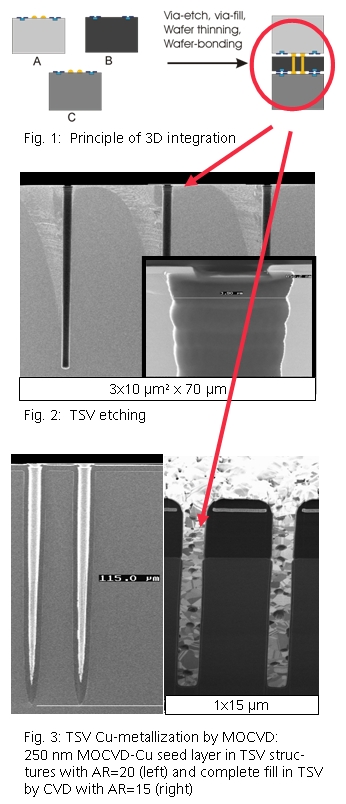
3D integration is of major interest for several applications in fields of microelectronics and MEMS technology. Hereby chips are stacked vertically to minimize electrical path lengths and thus enhance the electrical and thermal performance as well as to minimize the chip size. On the other hand, 3D integration provides the opportunity to integrate electronic devices of different functions and technologies, e.g. MEMS electronic devices of corresponding activation and evaluation electronics. The fabrication technology comprises processes such as wafer thinning, through-silicon via (TSV) drilling/etching, TSV filling and wafer bonding.
Research and development topics
We have been working in the field of 3D integration for several years with focus on the development of TSV etching processes and TSV metallization. For the full process chain Fraunhofer ENAS is collaborating closely with Fraunhofer IZM Berlin, IZM-ASSID Dresden and EMFT Munich.
TSV etching
The geometry of TSV’s has large impact on the subsequent filling with conductive materials. We are developing etch processes for optimized via profiles such as tapered openings.
- Aspect ratios up to 9
- Smallest TSVs: 3x10 µm² with depths up to 70 µm
- Tapered via opening with 86° top to sidewall angle
TSV metallization
The metallization scheme is the following:
- MOCVD TiN
- Deposition of adhesion layer (TiN-based)
- In situ MOCVD Cu (CupraSelect ™)
TSV’s with diameters smaller than 3 µm can be completely filled with Copper CVD. For larger TSV diameters Cu-MOCVD is used to deposit seed layers for Cu-electroplating. The results of all deposition processes are strongly influenced by the geometry and depth of the TSV’s and structure density. The processes should be optimized for each TSV layout for best compromise in deposition rate and step coverage.
Equipment
- AMAT PRECISION 5000 CVD-Tool for barrier and Cu-CVD
- Applied Materials P5000 DCVD (PECVD SiO2, SiN, SiC:H, SiCN:H, PE-TEOS, TEOS/Ozone)
- STS DRIE etching tool
- AMAT Mirra for barrier and Cu CMP
- IPEC472 for Si- and SiO2-CMP
Processes
 Fraunhofer Institute for Electronic Nano Systems