 Fraunhofer Institute for Electronic Nano Systems
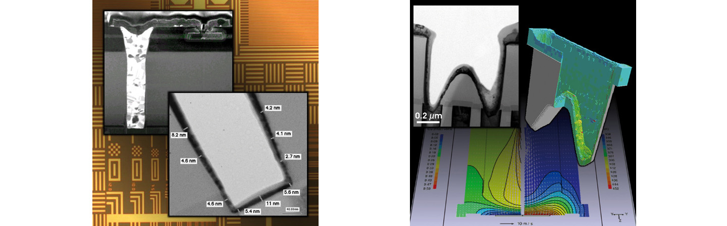
The focus of the department is on nano devices and nano integration technologies. Thereby, different business units of Fraunhofer ENAS are addressed, in particular Micro and Nanoelectronics and Sensor and Actuator Systems.
Process Technologies
Increasing diversification, the development of new devices and architectures leads to a larger material diversity and thus, to new integration and compatibility challenges for materials and processes. The topic nano process integration addresses i.a. the implementation of new materials and the development of new deposition processes for these materials such as atomic layer deposition (ALD). The integration into the overall technology, verification of material compatibility and stability with regard to the desired (electrical) functionality of the materials are focal points here.
With the electron beam exposure system Vistec SB 254, a very efficient industrial nanopatterning tool is available. Due to the flexibility regarding materials and substrate geometries, Fraunhofer ENAS has a unique selling point toward many other research institutions and semiconductor companies. Important application examples are the manufacturing of nanoimprint masters and optical components such as diffraction gratings, plasmonic nanostructures, metamaterials as well as micro and nanofluidic channel systems.
Furthermore, the department focuses on process technologies for the Back-End of Line (BEoL) and 3D integration.
Nano devices
The utilization of nano materials such as carbon nano tubes in novel electronics and sensor systems includes developments toward integration technologies in different systems (e.g. MEMS, MOEMS, AISC) compatible with silicon technologies, but also new technologies for flexible electronics. A nano technology platform has been established that provides basic functional elements such as carbon nanotube transistors with high integration density at wafer level for R&D and applications.
Memristors are also being developed, which enable digital and analog data storage and data processing but also digital and analog information processing for machine learning and artificial intelligence (AI) applications. This is based on preliminary works and in cooperation with the Helmholtz Center Dresden-Rossendorf (HZDR). To replace energy-intensive AI computers, AI is currently being integrated into energy-efficient general-purpose microcontrollers with trainable neural networks. In the future, AI is to be integrated into application-specific, analog electronic circuits with trainable neural networks and direct circuit-sensor interfaces. Thereby, the neural network is a crossbar circuit with memristors, which can both process and store data.
In the field of spintronics, Fraunhofer ENAS is mainly concerned with developing multidimensional and highly sensitive magnetic field sensors based on GMR (giant magnetoresistance) and TMR (tunneling magnetoresistance) effects and making them usable for various application environments. Application examples are i.a. measurement of the electric current and position/distance determination with special attention to the control of magnetic interference fields.
Simulation
The simulation of processes, equipment and devices supports the development of novel technologies by developing and optimizing the necessary processes and equipment. The focus is on the simulation of various deposition processes, the nanomaterials deposited with them and the simulation of nanodevices.
The department cooperates closely with the Center for Microtechnologies (ZfM) of Chemnitz University of Technology, the Fraunhofer Institutes of the Research Fab Microelectronics Germany (FMD) and the High-Performance Center Functional Integration of Micro and Nanoelectronics.