Fraunhofer Institute for Electronic Nano Systems
Electrochemical and Electroless Deposition (ECD & ELD)
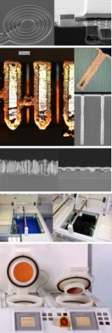
Electrochemical (ECD) and electroless (ELD) deposition of metals is used in microelectronics and MEMS technology as an alternative to CVD and PVD processes. The Fraunhofer ENAS in cooperation with the Center for Microtechnologies at the Chemnitz University of Technology is involved with ECD/ELD processes in basic research and industry related projects.
Research and development topics
ECD and ELD is used to fabricate interconnect metallization in microelectronics as well as metallization systems for MEMS components. One major topic in both cases is the metallization for packaging and vertical integration related issues, i.e. frames for wafer bonding or through-silicon vias (TSV).
Materials
The standard materials that can be deposited in ECD/ELD are:
- Copper ECD
- Gold ECD and ELD
- Nickel ECD and ELD
The process of the following materials is currently in development:
- Tin ECD
- Zinc ECD
- Pd ECD
Applications
Some typical applications of ECD and ELD are:
- Metallization systems for wafer bonding techniques
- Electronic components (microcoils)
- Thin film encapsulation
- TSV metallization
- Metallization on nanostructures
- Filling of sub-µm structures for interconnect applications
Equipment
We operate tools for basic research (rack plater, cup plater) and for industry related projects (fountain plater):
- Semiautomatic »fountain plater« tool for 100, 150 and 200 mm wafers (RENA EPM 201 F)
- Rack Platers with several ECD and ELD baths
- CVS analysis tool
- Rinser dryer