Fraunhofer Institute for Electronic Nano Systems
Challenges concerning process plasmas in terms of process reproducibility, chamber conditioning, or substrate quality are currently everyday business for semiconductor manufacturers. For example, the so-called "First Wafer Effect" still poses one of the greatest challenges. Particularly companies or institutes with a highly variable process mix in the same process chamber expend considerable effort to tune processes so that substrate quality remains consistent.
Another aspect lies in the quality assessment of processed or structured substrates. Especially in the manufacturing and development of semiconductor devices, it is rare that a comprehensive (often destructive) sample analysis is conducted after plasma processing.
The complexity of reactive ion etching seems to prevent access to solving such problems. The interactions between the plasma, the substrate, and chamber walls complicate the detailed prediction of process outcomes based solely on known process control parameters.
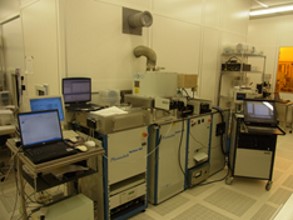
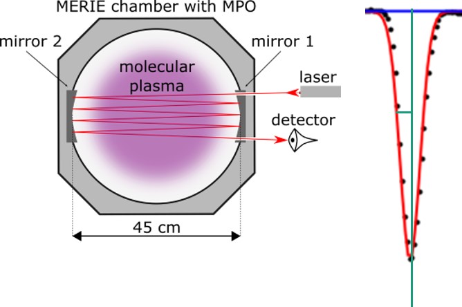
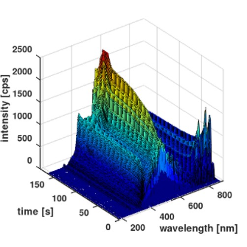
To address this issue, process plasmas at Fraunhofer ENAS are analyzed in situ.