

We have comprehensive experience in the area of the Chemical Vapor Deposition (CVD) of metals and dielectrics for different applications. Beside the use of established industrial processes and commercially available precursors, precursor evaluation, process development and optimization for the adjustment of the layers properties are executed. The current facilities enable plasma-enhanced as well as thermal CVD processes. The deposited dielectrics are suitable for the use in or between conductor paths of integrated circuits, as diffusion barriers, stop and hard masks for structuring, functional, cover and protecting, sacrifice or as tensed up layers for the increase of charge carrier mobility within the MOS transistor channel.
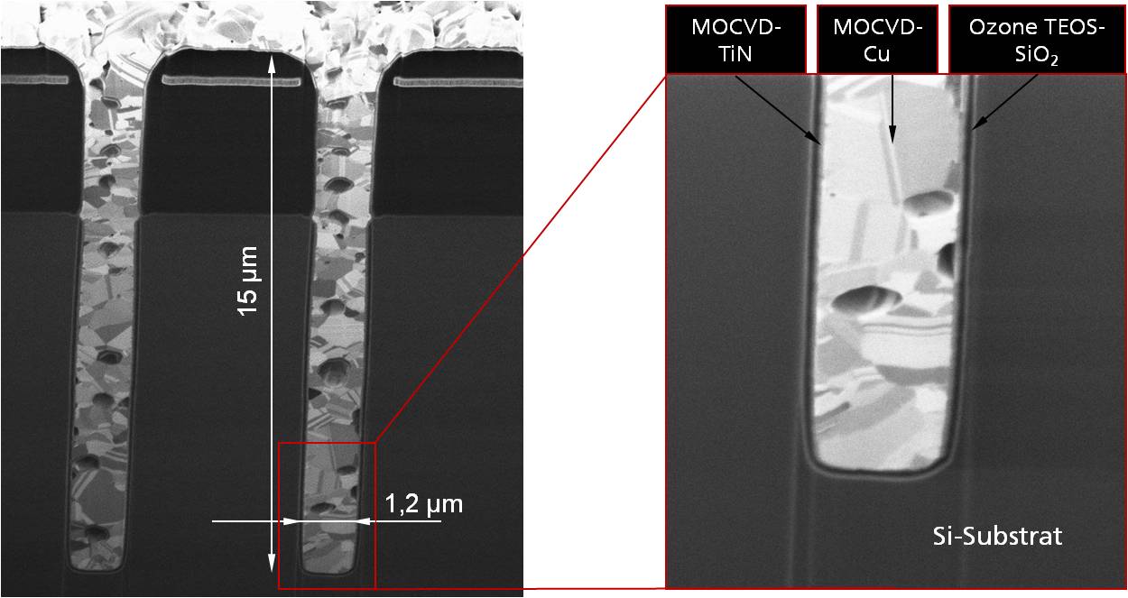
Depending on the application, the properties of the dielectric layers are adjusted. Process compatibility and integration of dielectric layers are as important as individual parameters, like electrical, optical, mechanical, and thermal properties, for this kind of investigations. CVD processes are additionally used for the metallization of interconnect systems as an alternative to Physical Vapor Deposition procedures or electroplating, for example in MEMS production for the 3D integration with Through Silicon Vias (TSV).
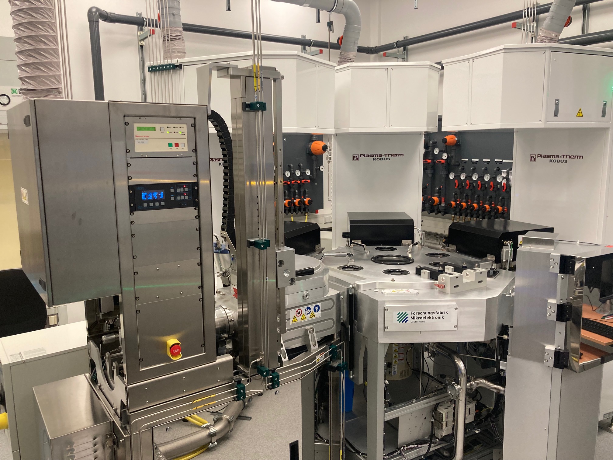
Our Plasma-Therm Kobus equipment for 200 mm wafers has four chambers: one for preclean/etching, and dedicated chambers for Co-, Cu- and TiN-CVD processes. The deposition of copper in a thermal MO-CVD procedure with the precursor CupraSelect™ is used for the formation of a copper seed layer for subsequent electrochemical processes and the metallization of TSVs or conductor paths. Titanium nitride is deposited with the help of the precursor tetrakis-(diethylamido)-titan (TDEAT). These layers are used for example as diffusion barrier for copper.
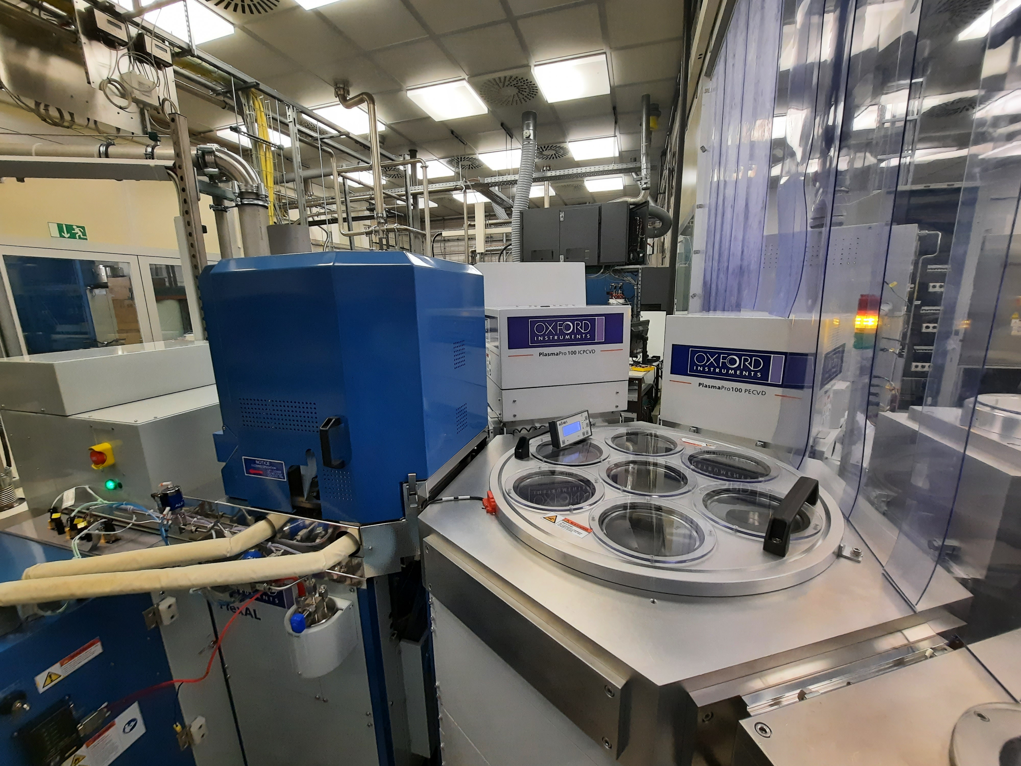
For the thermal or plasma-enhanced deposition of silicon oxide, silicon nitride and silicon oxynitride on 150 mm wafers a P5000™ equipment from Applied Materials is available. Furthermore, our Oxford cluster equipment with PlasmaPro 100 PE- (Plasma Enhanced) and PlasmaPro 100 ICP-CVD-chamber (Inductively Coupled Plasma) for 200 mm wafers enables the deposition of silicon oxide, silicon nitride and silicon oxynitride as well. For a good edge coverage a deposition procedure with tetraethyl orthosilicate (TEOS) is available.
Competency
- Plasma-enhanced and thermal CVD processes (e.g. PE-, ICP-, LP-, MO-CVD).
- Deposition of dielectrics, semiconductors and metals in variable layer thicknesses
- Development, optimization and application of CVD processes
- Precursor evaluation / precursor screening
- Wafer sizes up to 200 mm in diameter
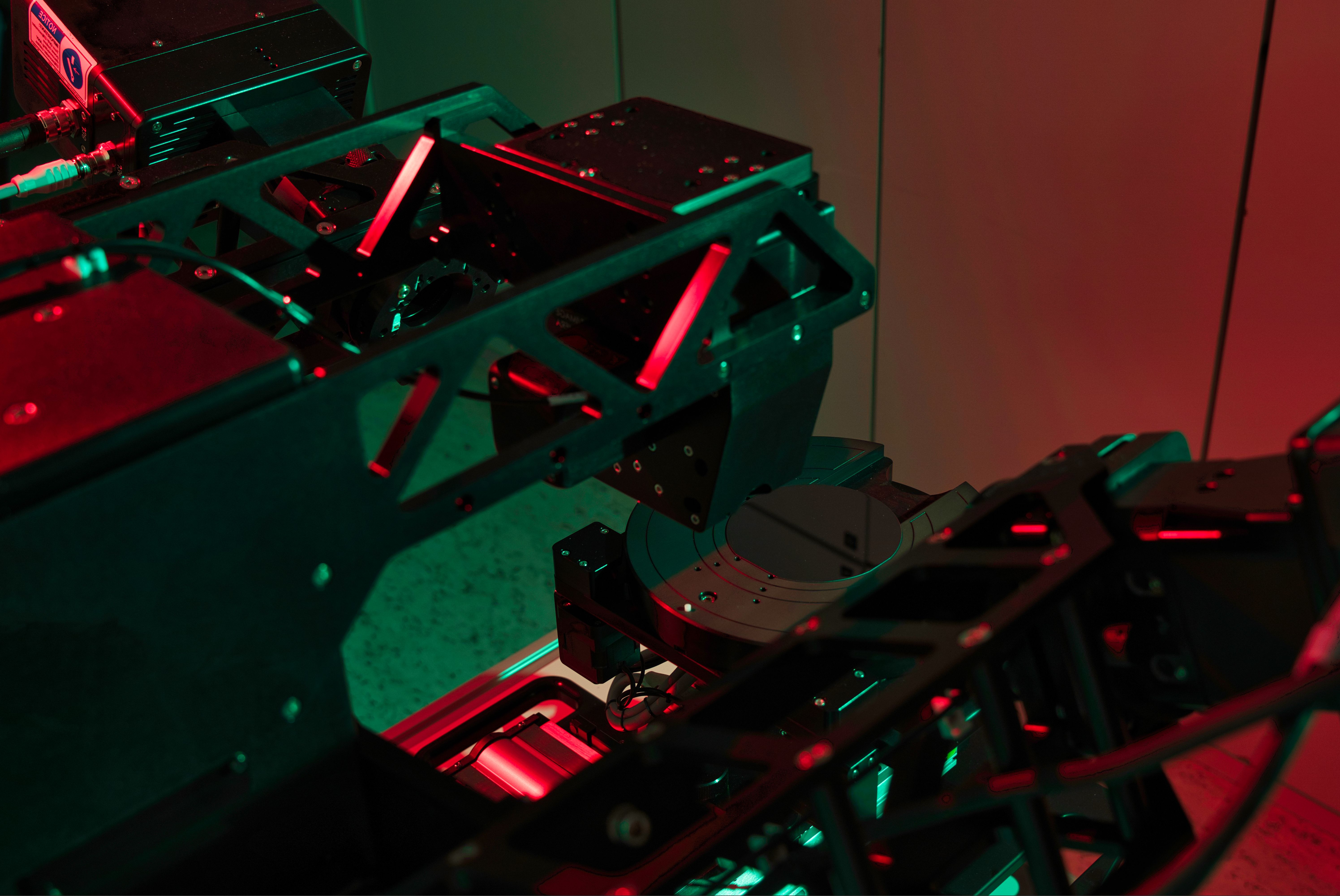
- Layer characterization by spectroscopic ellipsometry (Woollam RC2) and XPS
Available CVD processes:
- SiOx, SixNy, SixOyNz
- Cu, TiN, Co
- Poly-silicon
- CF-polymers
- DLC (diamond-like carbon)
- Parylenes (N, C, D, F, AF4)
- Carbon Nanotubes (SWCNT/MWCNT)
 Fraunhofer Institute for Electronic Nano Systems