 Fraunhofer Institute for Electronic Nano Systems
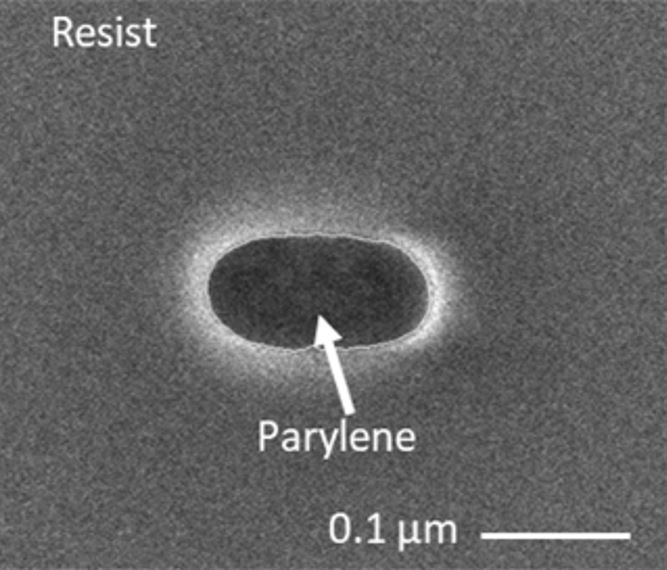
At Fraunhofer ENAS, in addition to the structuring processes typical for microelectronics, processes are also carried out, developed, and researched that cannot be performed without restrictions in industrially operated cleanrooms due to contamination reasons.
For instance, a copper structuring process using hydrogen-methane-based plasmas was developed at the institute. The successful structuring was performed on a reactor that operates based on the ICP principle.
The structuring of parylenes, for example for the manufacture and development of biosensors or technologies based on DNA origami, is also included in the institute's process portfolio.
Furthermore, CNTs are structured in our cleanrooms for the manufacture of, for example, pressure sensors, where a specially developed process sequence allows the targeted etching of CNTs.
Technology processes for aluminum nitride-based piezoelectric MEMS, among other things, require the dry structuring of platinum. The material is used as a seed layer to generate the desired crystal structure of aluminum nitride layers, so plasma etching of platinum is also among our processes.
Innovative technologies demand the development of new etching and structuring processes, which is why Fraunhofer ENAS continuously explores the feasibility of plasma-assisted structuring of various materials and consistently develops new processes.