 Fraunhofer Institute for Electronic Nano Systems
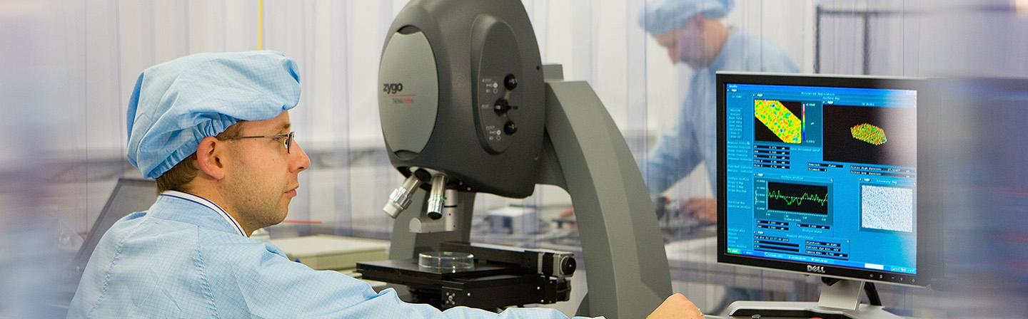
Test on chip and wafer level
The measurement of spatial parameters and mechanical stress is one of the biggest challenges in micro electro mechanical system (MEMS) test. Monitoring these parameters during the manufacturing process offers the possibility to react more quickly to process variations. Furthermore chips that do not meet the specifications can be selected even before the cost intensive packaging process has started. Often the production technology is very complex. A large number of sensors and other devices are fabricated in a wafer batch process. The biggest effort in manufacturing of MEMS is being caused by packaging and interconnection technologies, which also generate the major part of the costs of a device. Assuming a certain yield, a number of defective chips in addition to error-free will be assembled. Selecting these faulty devices before the packaging process can essentially reduce the costs of the entire MEMS product. Prerequisites are fast and reliable methods for wafer level testing of one hundred percent of the fabricated chips. These include the measurement of resonant frequencies, the determination and visualization of vibration mode shapes, as well as the identification of spatial parameters by combining measurement data with results from finite element analysis. Furthermore equipment and expertise for conducting surface, capacitance, insulation and resistance tests of MEMS are available.
MEMS test at wafer level is the main focus of the metrology group. The expertise ranges from surface, capacitance, isolation and resistance tests to the characterization of RF MEMS. Furthermore the measurement of resonant frequencies, the determination and visualization of vibration mode shapes, as well as the identification of structural parameters by combining measurement data with results from finite element analysis are carried out.