Press and News

Here you will find a list of the current press releases and news from Fraunhofer ENAS.

To directly receive information on forthcoming press releases and events, please register for our press distribution list via the following link: to registration.

In case you are looking for past events, please visit our archives.

Reset
  • © Fraunhofer ENAS

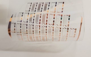
    If sounds seem increasingly muffled, if the outside world is getting quieter by the day, and if conversations become difficult to follow, especially when there is a lot of background noise, these are likely the initial stages of hearing loss. If left untreated, these early signs of hearing loss can lead to becoming completely deaf. Cochlear implants offer hope to people with severe hearing loss and deaf people to take a more active role in everyday life and access the world of sound. Current research efforts are focused on making progress in the field of technically assisted auditory perception with the aid of cochlear implants, which should enable improved speech intelligibility while at the same time ensuring a high level of patient comfort. The polymer Parylene, the innovative key component of these developments, is a real all-rounder, providing virtually invisible protection for the necessary electronics. At Fraunhofer ENAS, researchers such as Franz Selbmann are working on using this wafer-thin polymer to shield sensitive electronics for medical engineering and industry from external influences. In this interview, the scientist explains what makes Parylene unique and the potential applications of this advanced material, for instance for new generations of medical implants.

    more info
  • © Fraunhofer ENAS

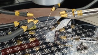
    It is difficult to imagine life today without a smartphone. Stowed within easy reach in our pockets and bags, these mobile companions are permanently by our sides and give us all the information and services we need to make our lives more convenient and enjoyable, whether we’re at home or on the go. All it takes is a click to immerse ourselves in a favorite playlist – making us feel transported back to last weekend’s gig right there in our living room – or share data in the form of vacation memories with friends and family in just a matter of seconds. Unique entertainment experiences can also be found in mobile gaming, which allows consoles to move away from the home PC and go anywhere, and ultra-fast video streaming for a movie theater atmosphere you can enjoy from the comfort of your sofa. The new 5G mobile network standard and its successor, 6G, will give all of these familiar services better and faster performance – but they are also set to make applications in autonomous driving, networked industrial automation and intelligent robot control a reality. There are certain essential technical foundations that need to be put in place to ensure that the mobile network can expand rapidly. A research team from Saxony in Germany is working together with Fraunhofer ENAS to achieve this. In the “KoVoPack” project, the researchers are laying the foundations for smart technologies that will soon allow users to benefit from higher maximum speeds, shorter response times and even more networking opportunities.

    more info
  • © Fraunhofer IIS

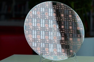
    On March 31, 2025, at the Hannover Messe, the Research Fab Microelectronics Germany (Forschungsfabrik Mikroelektronik Deutschland FMD) officially unveiled its new Chiplet Applica-tion Hub. Designed to serve as a central platform for the development and application of chiplet technologies, the hub aims to bridge the gap between research and industrial use. By working closely with industry partners, the hub accelerates the development of chiplets made in Germany, elevating industrial research to a new level. At the national level, it complements FMD’s role in the Chips for Europe Initiative, further reinforcing Germany’s technological resilience. The hub's research, development, and prototyping activities build on the infrastructure of the APECS pilot line, ensuring direct pathways to industrial application.

    more info
  • © Fraunhofer ENAS

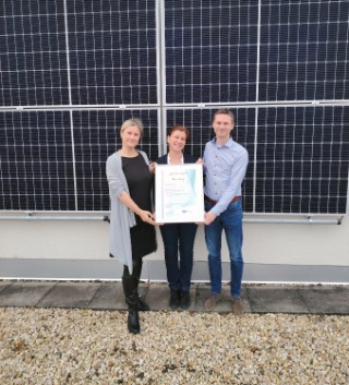
    Fraunhofer ENAS has been certified according to ISO 50001 since December 2024. The certification confirms the institute's commitment to greater sustainability and the responsible use of resources. With the introduction of the energy management system according to ISO 50001, Fraunhofer ENAS has implemented a structured framework that enables to continuously monitor and optimize energy consumption.

    more info
  • © Daniel Karmann / Fraunhofer IISB

    Silicon carbide (SiC) provides considerable technical advantages for power electronics - however, the costs are still a drawback. In the »ThinSiCPower« research project, a consortium of Fraunhofer Institutes is developing key technologies to reduce material losses and device thickness while increasing the thermomechanical stability of the assembled SiC chips. The savings achieved are expected to help further accelerate the market development of efficient SiC power electronics.

    more info
  • © ELES S.P.A.

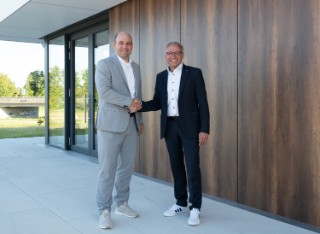
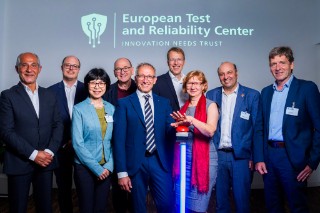
    The “Test and Reliability Center” (TRC) being built in the heart of Chemnitz, Germany, represents a research and development facility unique in Europe for testing and assessing the reliability of semiconductor components. Italian technology company ELES S.P.A., a leading provider of reliability testing equipment, has become a major initial working partner to the Fraunhofer Institute for Electronic Nano Systems ENAS during the center’s development phase. ELES S.P.A. will supply a state-of-the-art system for assessing electrical reliability, thereby creating ideal infrastructure conditions for the work of the TRC in helping the semiconductor industry to meet the highest quality standards in the future. The partnership will also jointly develop innovative automated testing methods for the chip industry.
    more info
  • State-of-the-art imaging procedures of radiological examination methods are indispensable in modern medical diagnostics. They open a window into the human body and make internal bone or tissue structures visible to detect diseases. As in medicine, researchers also regularly go in search of clues and use image-based diagnostic procedures from the field of radiology: by completely “illuminating” microtechnologies using X-ray radiation, they can bring to light hidden secrets that lie beneath the surface. At Fraunhofer ENAS, Elke Noack uses the non-destructive method to inspect electronic components with the utmost precision to detect defects. In this interview, the X-ray specialist explains how customers and partners can benefit from this expertise.

    more info
  • © Fraunhofer ISIT

    The pilot line for “Advanced Packaging and Heterogeneous Integration for Electronic Components and Systems” (APECS) marks a major leap forward in strengthening Europe’s semiconductor manufacturing capabilities and chiplet innovation as part of the EU Chips Act. By providing large industry players, SMEs, and start-ups with a facilitated access to cutting-edge technology, the APECS pilot line will establish a strong foundation for resilient and robust European semiconductor supply chains. Within APECS, the institutes collaborating in the Research Fab Microelectronics Germany (FMD) will work closely with European partners, to make a significant contribution to the European Union´s goals of increasing technological resilience, strengthening cross-border collaboration and enhancing its global competitiveness in semiconductor technologies. APECS is co-funded by the Chips Joint Undertaking and national funding authorities of Austria, Belgium, Finland, France, Germany, Greece, Portugal, Spain, through the “Chips for Europe” initiative. The overall funding for APECS amounts to € 730 million over 4.5 years.

    more info
  • © Fraunhofer ENAS

    On November 5, 2024, the Chamber of Commerce and Industry (IHK) Chemnitz awarded Fraunhofer ENAS the distinction of “exemplary vocational training organization,” honoring the institute’s long-standing commitment to training highly specialized young talent for the semiconductor industry.

    more info
  • © R-Tech GmbH

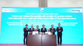
    The Fraunhofer Institute for Electronic Nano Systems ENAS in Chemnitz was joined today by guests from government and industry in celebrating the opening of its new “Innovation Office” at the “TechBase” innovation and start-up center in Regensburg, Germany. The move creates ideal conditions for the institute to expand its top-quality research services to include the south of Germany and develop forward-looking technologies in immediate proximity to customers and partners throughout the region.
    more info