 Fraunhofer Institute for Electronic Nano Systems
Service: Wafer bonding
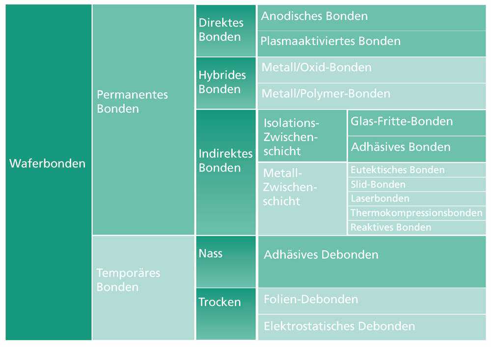
Wafer bonding is a process for temporary or permanent joining of two or more wafers with or without an intermediate layer. Wafer bonding has various applications: packaging (e.g. for sensors and actuators), assembly (e.g. for RF components), integration (e.g. for electrical/micromechanical/optical components), and substrate and device fabrication.
The System Packaging department offers standard wafer level bonding technologies such as silicon direct, anodic, glass frit, thermo-compression, and adhesive bonding. These technologies can be adapted according to the specific requirements (e.g. process temperature, yield, bond strength, and hermeticity) of target applications.
Regarding service of wafer-level bonding, clean rooms with fully integrated process line including characterization equipment for the processing of 4"to 8" substrates are available at Fraunhofer ENAS.