TSV reliability
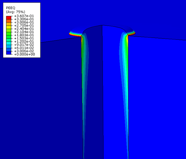
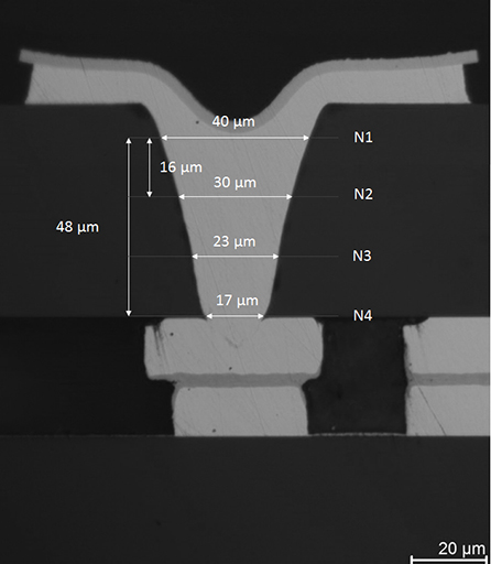
Copper Through silicon vias (TSVs) are an effective contacting solution for 3D integration but they also pose new challenges for thermo-mechanical reliability. The large mismatch of thermal expansion between copper and the surrounding silicon presents a significant risk of delamination between copper and the adjacent seed layer as well as of damage to Redistribution Layer (RDL) and back-end of line (BEoL) stacks on both sides of the silicon substrate. The resulting pumping and protrusion effects are evident both in the manufacturing of BEoL structures and during thermal cyclic testing (TCT). This is also due to changes in the copper morphology – grain size, grain orientation – as an annealing effect. For this purpose, extraction of mechanical properties from nanoindentation experiments were performed. Finite elements simulations to investigate the thermo-mechanical behavior of damage processes affect possible delaminations between the copper TSV and the barrier and also within the BEoL stack under TCT and CPI (chip package interaction) conditions. A CSM procedure (Cohesive Surface Contact Method), in combination with a traction separation law to describe the damage progress, was used to take the crack formation of bimaterial interfaces into account. Simulation results show interface delamination risks at the copper-seed interface close to at the upper end of the TSV. The evaluation of the interaction of TSVs and BEoL stacks using damage mechanics provides a good basis for damage initiation studies within the RDL and BEoL stacks on the top and bottom of the silicon substrate. Based on simulations of the dependence of the damage risk on the distance between the TSVs as well as the crystal orientation of silicon versus pairs of TSVs, proposals for a reliable via design were submitted.
 Fraunhofer Institute for Electronic Nano Systems
