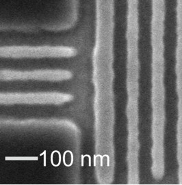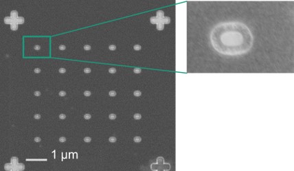


At Fraunhofer ENAS, a Vistec SB254 shaped beam writer with 50 kV acceleration voltage and 12 A/cm² current density is available for electron beam lithography. This allows for the realization of nanostructures up to 40 nm wide on various substrates for a variety of applications, such as:
- Optics
- Photonics (optical gratings, 2.5D and 3D structures, grayscale structures)
- Micro-/nanoelectronics
- Micro-Electro-Mechanical Systems (MEMS)
- Nano-Electro-Mechanical Systems (NEMS)
- Micro-Opto-Electro-Mechanical Systems (MOEMS)
- Mastering/Master fabrication for Nano-Imprint Lithography (NIL)
Processable substrates include:
- 4“, 6“, 8“ Semi Std. Si or GaN wafers
- 4“, 6“, 8“ wafers with thicknesses ranging from 0.5 mm to 1.5 mm
- Transparent substrates
- Other substrates upon request
Depending on customer needs and specifications, various resist systems (positive and negative resists, etc.) are used to optimally meet the requirements for dry etching or lift-off applications. The necessary layout adjustments, optimizations in exposure, and etching are performed in-house to be optimally coordinated.
The execution of overlay exposures with alignment to global marks and chip marks is an essential part of our work and is often used for transistor applications where source-drain and gate must be optimally aligned.
Furthermore, the use of Nano Imprint Lithography (NIL) for nanoscale structure sizes can also realize cost-effective production for a larger number of wafers. Mix and match exposures of electron beam and UV projection exposure also provide an option for efficient exposure times for the realization of nanostructures.
 Fraunhofer Institute for Electronic Nano Systems