
Electrochemical Deposition (ECD)

Business Unit »Process, Device and Packaging Technologies«

Electrodeposited aluminum bond frames with > 5µm layer thickness for thermocompression bonding.
© Fraunhofer ENAS
Electrodeposited aluminum bond frames with >5 µm layer thickness for thermocompression bonding
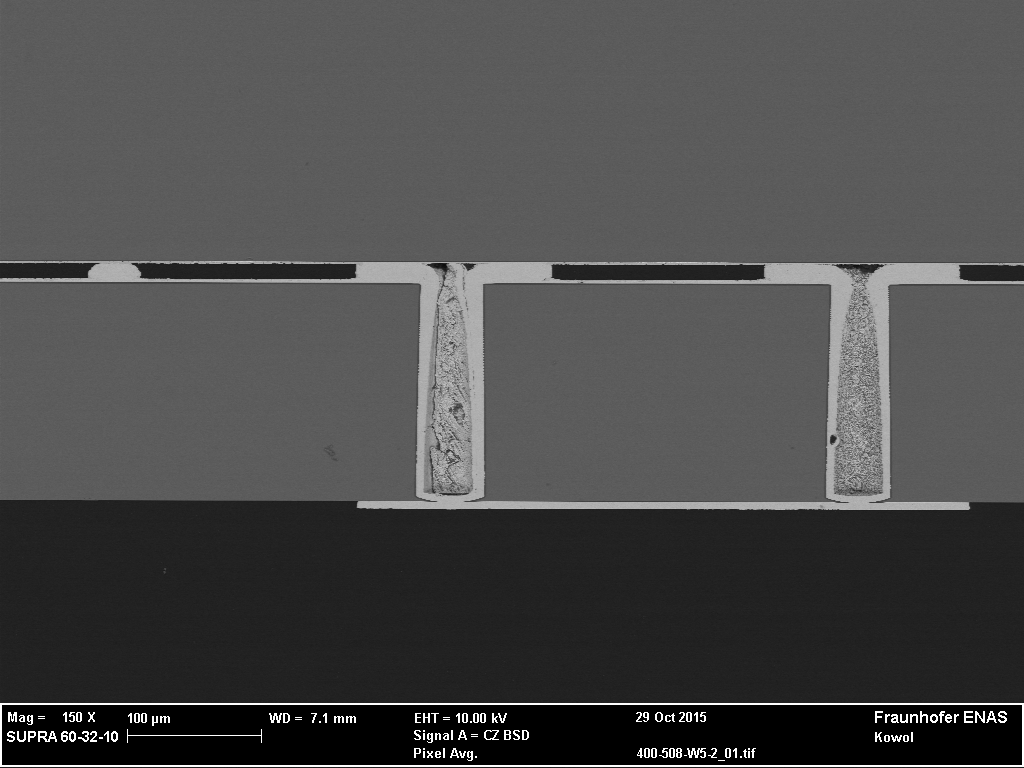
Conformal coating of through silicon vias for 3D integration of MEMS.
© Fraunhofer ENAS
Conformal coating of through silicon vias for 3D integration of MEMS.
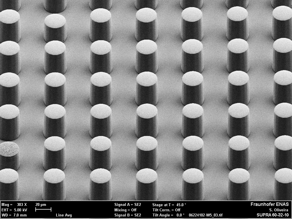
Copper pillars with 30 µm diameter and 50 µm pitch (can also be produced with gold or aluminum).
© Fraunhofer ENAS
Copper pillars with 30 µm diameter and 50 µm pitch (can also be produced with gold or aluminum).

Electroplating

The electroplating of metals and metal alloys is used as a complement for CVD and PVD processes in microelectronics and MEMS technologies. Electroplating is capable of creating layer thicknesses in the range of one to several ten microns. In cooperation with the center of micro technologies of TU Chemnitz, the Fraunhofer ENAS is working on fundamental, applied and industrial research.

Research and Development

ECD is widely used to produce conductive paths in microelectronics and in MEMS components. Some significant aspects here are the Damascene technology, deposition of bonding layers (wafer bonding, chip bonding) as well as the metallization of through silicon vias (TSV) for the vertical integration of components.

Besides the water-based deposition, the electroplating from ionic liquids is also studied. The focus of research is Aluminum electroplating for applications in microelectronics, microsystem technology and in printed circuit board technology. Fraunhofer ENAS is proficient in aluminum electrodeposition on 150-mm wafers on different seed layers (Al, Cu, Au, Pt) and highly doped silicon. It can be used as electrical and thermal conductive material as well as bonding layer for wafer and chip level bonds.

Materials and Applications

Application

material

materials in development

Substrate size

Intermediate bonding layer

Cu, Al (ILs),  Au, Sn, SnAg

Au80Sn20, In, Ga

100…200 mm

Al: 150 mm

Interconnects, Through Silicon Vias (TSVs)

Cu

Al (Ils), Au

100…200 mm

Al: 150 mm

Damascene

Cu


100…200 mm

Redistribution layer

Cu, Au, Al (ILs)


100…200 mm

Al: 150 mm

Micro patterns (i.e. micro coils, interdigital electrodes)

Cu, Al (ILs), Au


100…200 mm

Al: 150 mm

Bumping (UBM, pillars, solder bumps)


Cu, Au, Sn, SnAg

Al (ILs), Au80Sn20, In

100…200 mm

Al: 150 mm

Multi layer systems for reactive bonding


Pd/Sn

Not on wafer level yet


Equipment

  • Full-automatic Fountain Plater Solstice S4 (ClassOne)
  • Semi-automatic fountain plater for 100…200 mm wafers (RENA)
  • Semi-automatic vertical deposition tool for 100…200 mm wafers (Ramgraber)
  • Plating Unit and glovebox for ionic liquid based ECD (Silicet AG)
  • Mobile Plating Unit for low electrolyte volume tests,e.g. Au80Sn20 (Silicet AG)
  • Basic research with a Hull cell or in a beaker
  • Different pulse plating power sources (plating electronic, Munk) and a potentiostat VersaSTAT 3 (Princeton Applied Research)
  • Analytics of organic and inorganic electrolyte components using CVS (Cyclic Voltammetric Stripping) and gravimetric titration

ECD technical details