UNSETH: process and reliability assessments of integration and packaging technologies providing hardware-based security


Security has become a vital part of European electronic equipments as they handle sensitive data in uncontrolled environments and increasingly face content protection issues and counterfeiting. Tamper protection and high security, compatible with mass production cost and robust secure protection for high-end products, are focused on within the EU project UNSETH (FP7-SEC GA N°312701). It adds new tamper detection features and higher tamper resistance for electronic assembly and packaging to yet available chip level solutions and proposes a generic protection profile up to the highest possible assurance level.
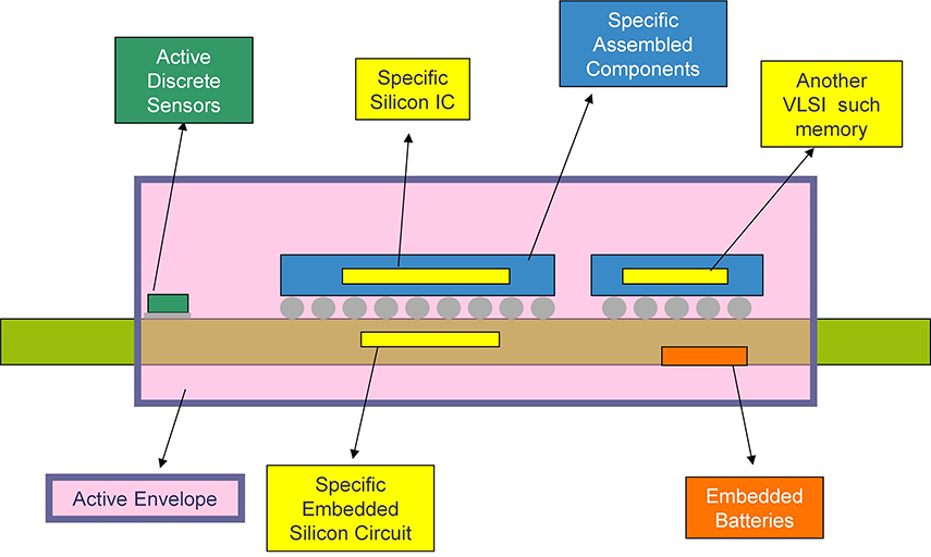
By introducing new nanomaterials printed envelope, 3D devices and mesh embedded into PCB and SiP with active anti-tamper sensors or combination of all, testing and reliability evaluation, UNSETH provides advanced secure systems. Both, the electronic modules themselves and manufacturing processes are under development including aerosol jetting of nanoparticle inks at Fraunhofer ENAS, components embedding in PCB at AT&S and eWLP and SiP assembly at Nanium. Thales checks manufacturability of the technologies and brings in security applications for which Epoche & Espri proposes the protection profiles.
Two complementary technologies set up tool boxes for security:
1st level of anti-tamper protection by embedding protectable secure microcontroller in PCB as highly integrated part of the electronic system
2nd level of anti-tamper envelope by a secure sensor printed in a casing above the electronic module
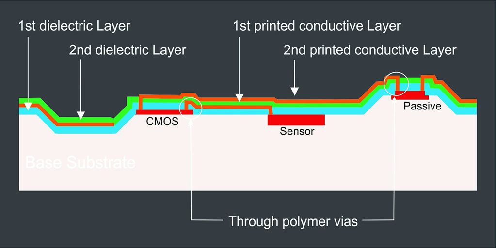
At Fraunhofer ENAS, a new 3D integration approach based on printed multilayers and through-polymer vias was developed for the secure envelope and to enable vertical and horizontal integration of components, different in shape, size, material, process and function combining multifunctionalities in one package and miniaturizing smart systems. A parylene thin film is insulating conductive multilayers with interconnect vias opened by a fine-tuned laser ablation process. For conductive multilayer fabrication entirely basing on aerosol-jet printing (AJP) technique, Fraunhofer ENAS explored the printing of a commercially available silver nanoparticle ink on a CVD parylene dielectric coating and via filling. AJP enables < 20 µm fine line deposition of metal particle inks strongly depending on used ink, substrate materials and pre-treatment. Highly conformal homogeneous void free coatings with good insulation properties even on 3D substrates achieved by the CVD process in vacuum close to RT, pre-treatment procedures, AJP of Ag ink and opening vias in parylene by laser ablation without damaging the layers underneath demonstrate a new approach for multilayer redistributions on substrates with some level of 3D form factor.
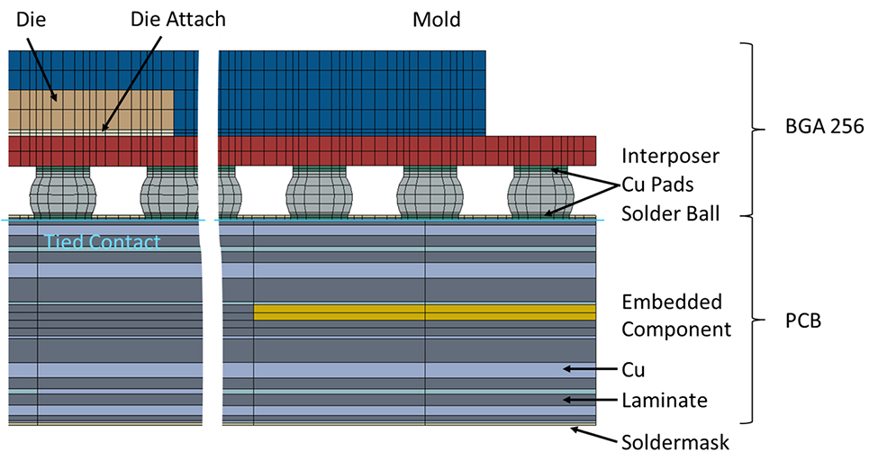
Reliability assessments of smart secure PCB in presence of both, embedded components as well as large SMD, used FE models to evaluate thermo-mechanical stresses and strains numerically. Simulations of process and test steps and related experiments located and monitored stresses, plastic and creep strains evolving in the embedded dies and interconnects, primarily induced by CTE mismatches between PCB and components. Temperature cycles, vibrations, shocks, etc. pose risks for modules within systems of high security relevance. Detailed local 3D models thus replicated corresponding physical effects, always calibrated experimentally in reliability tests for evidence of failure mechanisms, locations and probability. To evaluate solder joint degradation as well as delaminations and cracks between the PCB and embedded components in detail, a global/local modeling strategy was followed for identifying loading conditions mainly contributing to degradation and for minimizing excessive stressing of the device.
 Fraunhofer Institute for Electronic Nano Systems