Simulation of devices based on carbon nanotubes

Carbon nanotubes (CNTs) are promising materials for future electronic devices due to their extraordinary mechanical strength in combination with excellent electronic and thermal properties. Technological concepts for the wafer-level integration of CNTs for sensor, transistor, and interconnect applications are currently developed at Fraunhofer ENAS and the Center for Microtechnologies Chemnitz (ZfM).
The functionality of CNT-based devices is often governed by quantum effects. Properties depend strongly on the dimensions and structural details at the atomistic level. Thus, along with the technology developments, adequate simulation concepts are required. Ab initio methods for the description of quantum effects have to be applied and linked to numerical device simulations, from which compact models for the circuit simulation can be derived. During the last years, methods for the simulation of nanodevices have been established at Fraunhofer ENAS in close cooperation with the more fundamental work groups at the ZfM. As an example, the contact properties of CNTs with various metals have been studied systematically.
A new tool for the efficient simulation of large quasi 1D structures: CNTs with structural defects
CNTs used in applications are never defect-free. Thus, a thorough understanding of the influence of defects on the performance of potential CNT-based devices is required.
In a recent study we have analyzed the influence of structural defects on the electronic transport in metallic CNTs. The study focuses on CNTs with a length of up to several microns and a very high number of defects. This is a big challenge for quantum simulation methods like DFT, where the computational effort is proportional to the 3rd power of the system size (or worse). Based on the recursive Green’s function approach, a linear scaling simulation tool was implemented at Fraunhofer ENAS, which allows us to study systems of realistic size with quantum mechanical accuracy. The approach is very general and can be applied to various kinds of quasi one-dimensional structures like CNTs, nanowires or polymers.
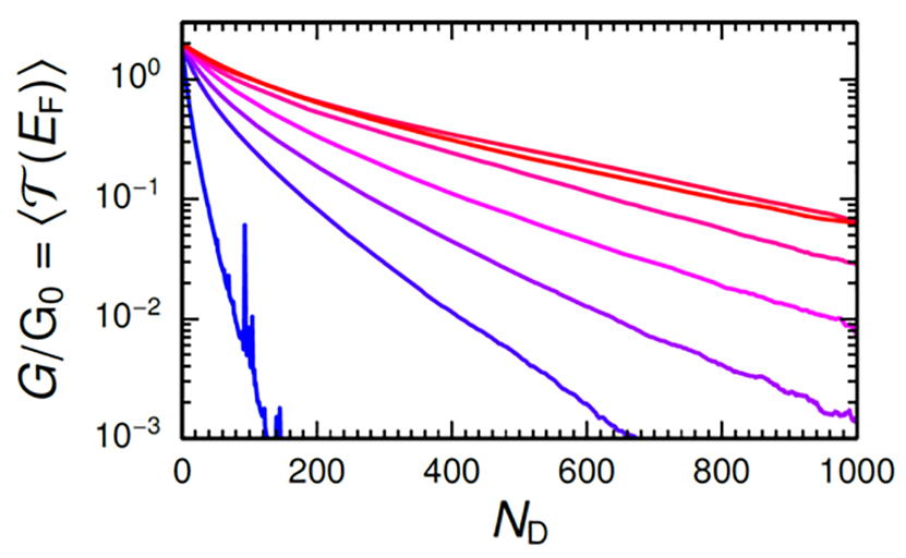
Our work shows that the electron transport in CNTs with a high number of randomly arranged defects is in the regime of strong localization, where the conductance decreases exponentially with the number of defects. This is characterized by an exponential prefactor, which depends on the defect type, CNT diameter and temperature.
Device simulation of CNT FETs-based on quantum transport simulations
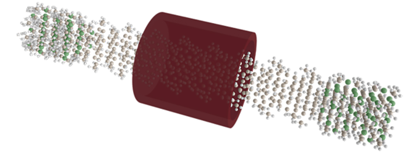
A simplified device model has been used to study doped CNT FETs with a channel length in the order of 10 nm (close to prototypes @ IBM) surrounded by a cylindrical gate. The software Atomistix ToolKit is used for the quantum transport simulations. The underlying electronic structure calculations are based on a semiempirical extended Hückel model with parameters that describe the transport in CNTs with DFT-like accuracy.
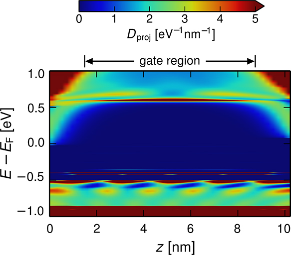
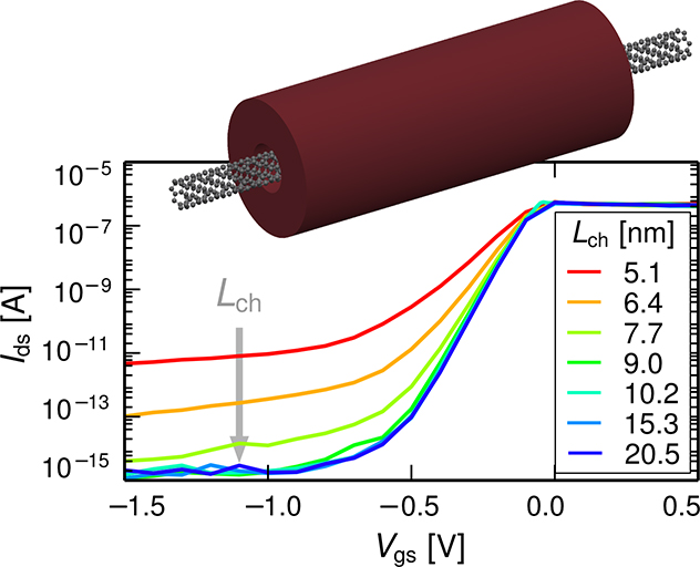
Transfer characteristics of CNT FETs with different channel- and gate lengths are obtained from a series of device simulations. All the simulated transistor configurations show very good switching behavior and very high on/off-ratios. A remarkable finding is the fairly good transistor performance even for extremely short gates of 0.4 nm. The best devices reached on/off-ratios of 107. By analyzing the spatially resolved density of states, we see that the band edges of the valence bands are fixed due to the presence of localized states within the gate region. This suppresses band-to-band tunneling and enables the excellent device performance.
 Fraunhofer Institute for Electronic Nano Systems