Simulation of mechanical strain in 22 nm FDSOI devices


Fully depleted silicon on insulator (FDSOI) is the European approach for ultra-scaled energy efficient microelectronic circuits. Within the WAYTOGOFAST project, which is a part of the European initiative ECSEL, a big industry driven research consortium explores FDSOI devices at the 22 nm technology node and beyond.
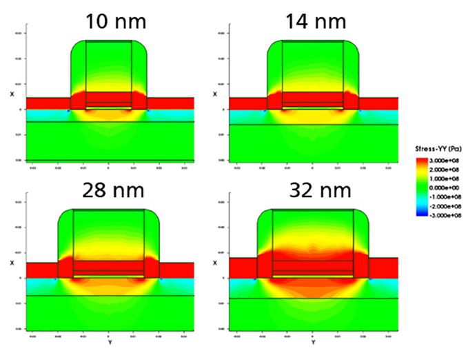
Strained transistor channels are used to increase the charge carrier mobility. Engineered channel strain is thus one of the key factors to obtain high performance energy efficient FDSOI devices. Many factors like device geometry, details of the process flow as well as pre-strain of the ultra-thin silicon layer on the wafer influence the actual strain level in the transistor channel. Researcher from ENAS worked on modeling and simulation of strain in 22 nm FDSOI devices. The strain simulations provide unique insights into the interplay of mechanics and electronics inside the nanoscale devices. We could identify several key parameters, which have a drastic influence on the strain level and thus on the device performance. By using the opportunity to explore huge parameter spaces, we could show that process-induced variations occurring during the device fabrication can give rise to severe strain induced performance loss.
 Fraunhofer Institute for Electronic Nano Systems