Atomic Force Microscopy

Automatic AFM (Atomic Force Microscope)

Bruker InsightCAP AFM
© Bruker
Bruker InsightCAP AFM
Profile measurement with a measuring length of 7 mm, topographical unevenness can be detected
© Fraunhofer ENAS
Profile measurement with a measuring length of 7 mm, topographical unevenness can be detected
Microlens array measured with DT mode
© Fraunhofer ENAS
Microlens array measured with DT mode

Bruker InsightCAP

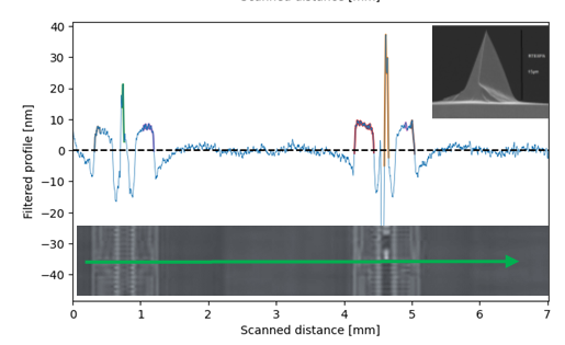
Using AFM, surface structures and properties can be depicted at the nm and sub-nm scale.

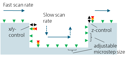
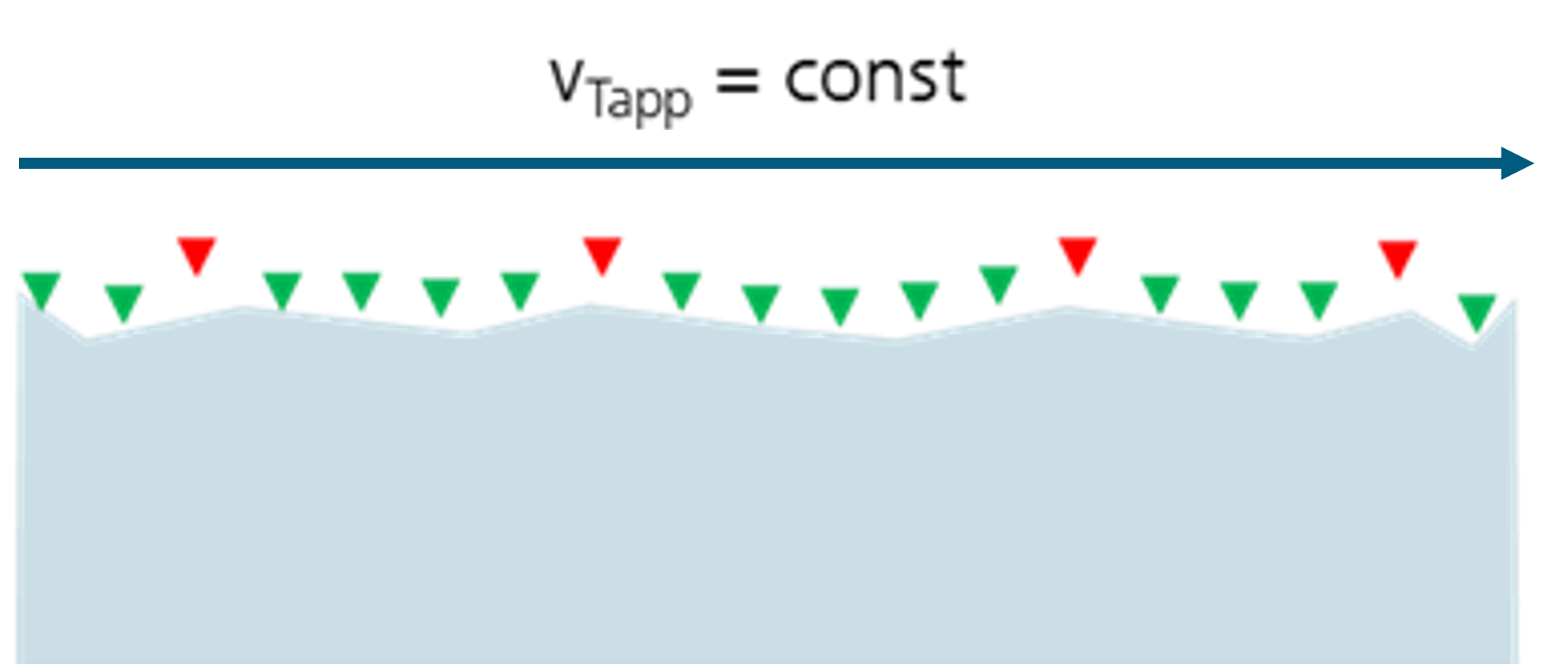
In general, in an atomic force microscope, a microscopic tip with a tip radius of ~10-50 nm is attached to a cantilever. When the tip is brought close to the examined surface, an attractive or repulsive interaction between the surface and the tip occurs. The force is transferred through the tip to the cantilever, causing the cantilever to deflect. Using piezo crystals, the tip can be moved in all three spatial directions, enabling the scanning of surfaces in a grid-like manner.

The Bruker InsightCAP is a fully automatic AFM. This allows high measurement throughput, statistical process control and comprehensive analysis of production batches.

The InsightCAP features the following:

  • Automatic measurement system for 4", 6" and 8" wafers
  • Recipe-based automatic measurements, including mark recognition, the measurement itself and also automated evaluation
  • High accuracy and repeatability
  • Integrated tip management / qualification system, allowing the continuous monitoring of the tip condition, even in case of a high measurement volume
  • Wide range of tips and measurement methods facilitate a broad area of application
    • Tapping mode
    • Profiling
    • Topography mode
    • Critical dimension (CD)

Tab navigation

Roughness measurement of a polished SiO2 surface (Ra ~ 0.2 nm)
© Fraunhofer ENAS
Roughness measurement of a polished SiO2 surface (Ra ~ 0.2 nm)
Roughness measurement of a metal surface after deposition (Ra ~ 12 nm)
© Fraunhofer ENAS
Roughness measurement of a metal surface after deposition (Ra ~ 12 nm)

Tapping mode is suitable for topography measurements < 20 nm.

This includes, for example:

  • Roughness measurements of polished surfaces
  • Roughness measurements for the characterization of metal layers
  • Analysis of hybrid bond surfaces, i.e., the depression of Cu vias compared to the SiOsurface to be bonded (= dishing)

Measurement specifics:

Data points are recorded at equal intervals in tapping mode, depending on the number of points, measurement field size, scan speed, and number of lines. These settings are global, and the data points are recorded independently of the position of the measuring tip relative to the surface. Therefore, this method is not suitable in the case of larger topography differences, as these can lead to defects in the measurement.

Dishing measurement of copper vias for hybrid bond surfaces
© Fraunhofer ENAS
Dishing measurement of copper vias for hybrid bond surfaces

Measurement example DT mode: Microlens array
© Fraunhofer ENAS
Measurement example DT mode: Microlens array
Measurement example DT mode: Vias (200 nm deep; 500 nm wide).
© Fraunhofer ENAS
Measurement example DT mode: Vias (200 nm deep; 500 nm wide)
Measuring principle DT mode
© Fraunhofer ENAS
Measuring principle DT mode

To measure surface topographies > 20 nm and for structural surveying, the deep trench (DT) mode is suitable.

This includes, for example:

  • Vias, trenches, ridges
  • 2.5D structures, such as microlenses or pyramid structures
  • Optical metastructures

Measurement specifics:

Unlike in tapping mode, in DT mode the spacing of data points can be set separately for horizontal and vertical structure directions. This increases point density in relevant areas.

Furthermore, data points are only recorded when the measuring tip is in a good position relative to the surface. This is achieved through regulation in the z-direction. As a result, the system can "respond" to the topography, and the measurement precision is significantly improved.

Measurement example CD mode: optical nanogrid. The system measures the structure on the surface and side wall and automatically evaluates the structure width at three points (blue, red, green). A special CDR tip is shown in the bottom right-hand corner.
© Fraunhofer ENAS
Measurement example CD mode: Optical nanogrid. The system measures the structure on the surface and side wall and automatically evaluates the structure width at three points (blue, red, green). A special CDR tip is shown in the bottom right-hand corner.

The critical dimension (CD) mode offers the same capabilities as the DT mode. The point density can also be varied here, separately for horizontal and vertical structure directions.

However, in this measurement mode, the measuring tip is adjusted not only in the z-direction of the surface but also in the x/y-direction. This allows for the recording of measurement points on vertical structures. This enables applications such as:

  • Measurement of sidewall roughness
  • Measurement of negative profiles (undercuts)
  • 3D imaging of the surface

This measurement mode requires special tips with a flared area at the tip to record data points directly on the sidewall.

© Fraunhofer ENAS
CD mode: The measurement principle and special AFM tip enable measurements on vertical structures
CD mode: Measuring principle and special AFM tip enable measurements on vertical structures
© Fraunhofer ENAS
CD mode: Measuring principle and special AFM tip enable measurements on vertical structures

© Fraunhofer ENAS
Profiling mode

The profiling mode is a special form of the tapping mode.

Scan lengths in the x/y-direction of up to 100 mm are possible, with simultaneous nm resolution in the z-direction.

This results in the following measurement applications:

  • Determining layout-related topography
  • Determining CMP-relevant parameters (e.g., erosion)