Inline Metrology CD-SEM Hitachi CS4800
For statistical SEM examinations, a Hitachi CS4800 CD-SEM is available for imaging 6" and 8" wafers of varying wafer thicknesses (275 µm to 825 µm). These wafers are loaded directly from the pod, allowing efficient characterization of large quantities (e.g., 40 wafers per hour at 5 measurement points per wafer). Transparent substrates can also be handled and imaged. With a resolution of up to 2 nm, images can be taken according to variable needs with a 4000x - 300,000x zoom. Reproducibility is 1 nm/3 sigma or 1%. Alignment and focusing are fully automated, as is the image analysis using image recognition, thus allowing for rapid statistical characterization across the entire wafer.
Highlights:
- Statistical SEM investigations and evaluation at wafer level
- 6" (wafer thickness 275 µm to 775 µm) and 8" (wafer thickness 725 µm ± 100 µm) wafers made of silicon and glass
- Special substrates on request
- Resolution up to 2 nm
- Automated measurement programs and analyses
- Defect review package / KLARF / KRF interface for targeted analysis of already known defects
- Microscale with 100 nm pitch

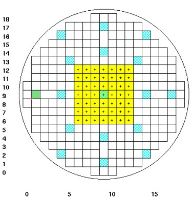
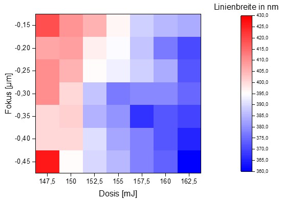
Wafer map on the CD-SEM. In the yellow-labeled array with 7 x 7 chips, fully automated measurements of the structure line width were performed. Due to a dose variation over different columns as well as a focus variation over different rows, the line widths vary depending on the position on the wafer.

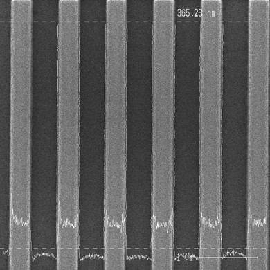
CD-SEM image of several line structures with automated measurement of the line widths. The value at the top of the image represents the mean value over the line widths measured on four lines in this example.

Aus den Messdaten erstellte Wafermap, aus der die Linienbreiten in Abhängigkeit von der Dosis und des Fokus abgelesen werden können.
 Fraunhofer Institute for Electronic Nano Systems