Fraunhofer Institute for Electronic Nano Systems
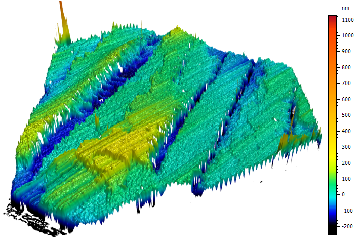
Fundamental processes in semiconductor and microtechnology include subtractive methods (wet and dry etching), additive methods (e.g., electroplating or printing techniques) and surface processing (wafer grinding, CMP). These processes result in intended and unintended topographies, roughness, and surface defects. Target structures, such as bond frames for wafer bonding or cavities in MEMS components, require precise determination of their structural height/depth and lateral dimensions. For unintended topographies and surface effects, which need to be leveled using chemical mechanical polishing (CMP), precise control of step height and surface roughness is essential.
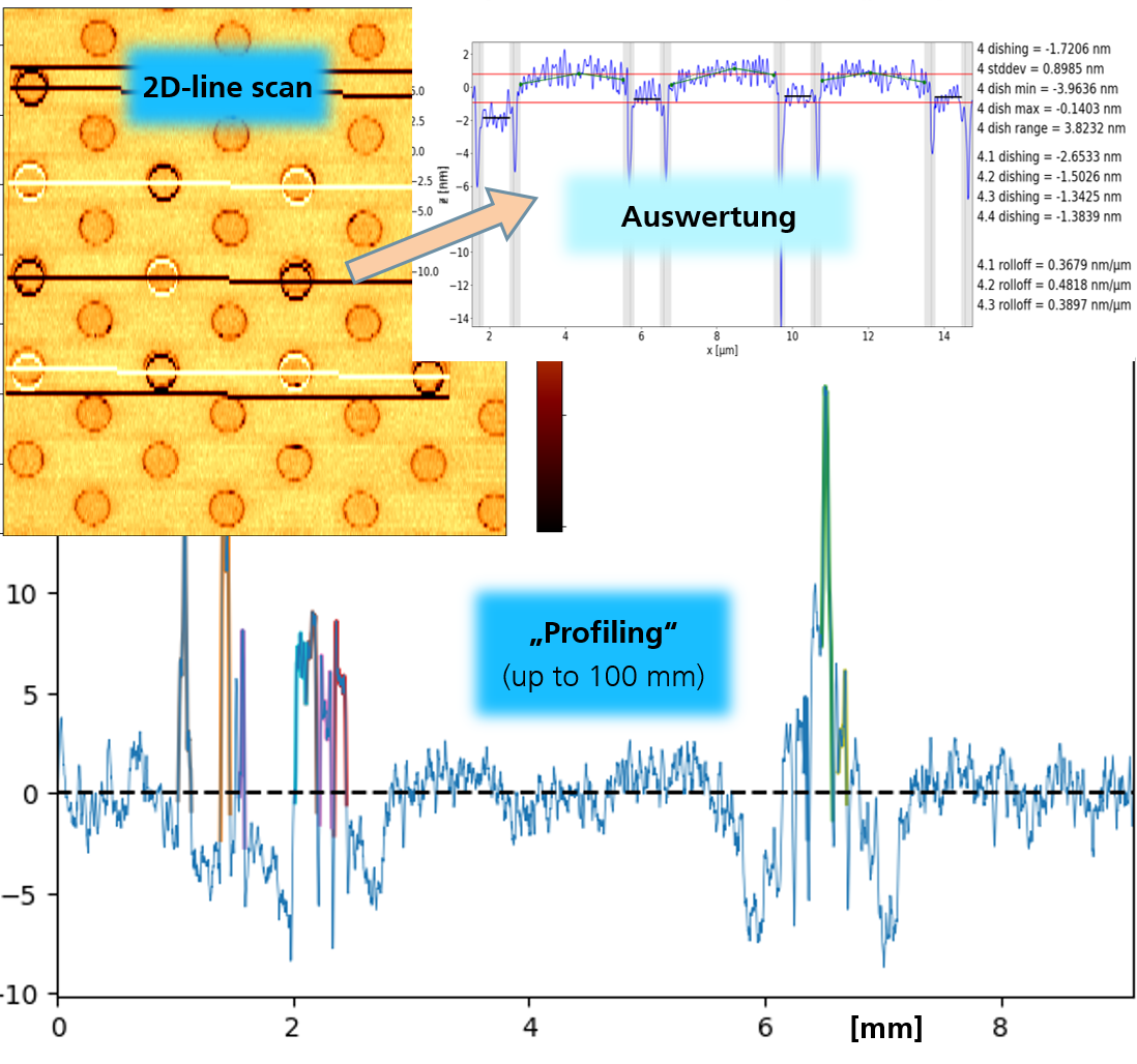
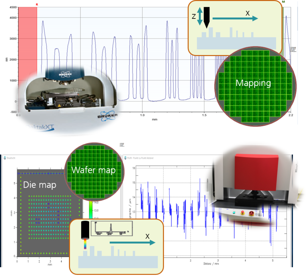
Profilometry is the key tool for achieving the aforementioned measurement tasks and can be essentially divided into tactile and optical methods, as well as atomic force microscopy. Fraunhofer ENAS employs the following methods as part of its inline metrology analytics. In addition to individual point analysis, these methods offer the possibility of fully or semi-automatic wafer mapping.
- Tactile profilometers (Dektak XT, 2x Dektak 150 Veeco)
- Optical profilometers using 2D or line scans (FRT dichromatic sensor)
- Planar 3D microscopy using confocal principle or focus variation (Confovis CL200, Confovis AOI 305, unity 4See BF3D)
- Nanoscale 2D scans and "long scans" using AFM (up to 100 mm, Bruker Insight Cap – fully automatic AFM)