Defect Inspections via Brightfield and Darkfield Analysis

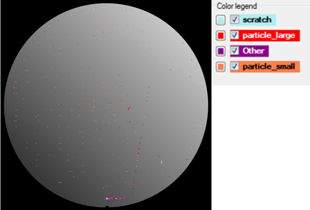
BF2D inspection, defect classification (left), this quality control (right).
© Fraunhofer ENAS
BF2D inspection, defect classification (left), dies quality control (right)

Brightfield and darkfield analyses are crucial procedures in the semiconductor industry to inspect defects on wafer surfaces and to control the quality of semiconductor devices.

Our defect inspection tool, Unity4See, combines these two types of optical inspection in a fully automated analysis device that can inspect 4", 6", and 8" wafers.

In brightfield inspection (BF2D – brightfield, 2D), a light source illuminates the surface of a structured wafer, which is then scanned column by column and the reflected light is detected. This enables the detection of >1 µm defects, such as layout errors, particles and scratches on the entire wafer surface.

LS defect visualization of particle agglomerations on bare wafer surface.
© Fraunhofer ENAS
LS defect visualization of particle agglomerations on bare wafer surface

The Unity4See lightspeed (LS) inspection technology combines dark-field inspection and synchronous Doppler detection to automatically detect spherical objects with a size of 90 nm.

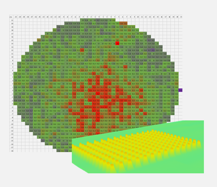
BF3D structural representation incl. height mapping.
© Fraunhofer ENAS
BF3D structural representation incl. height mapping

By combining this with 3D brightfield analysis (BF3D – brightfield, 3D), it provides additional detailed information about the topography, surface structure and defects of wafers.

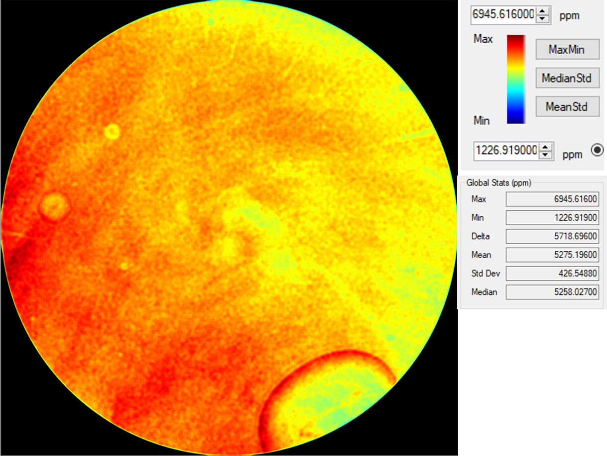
LS defect display, Haze wafer with rough surface
© Frauhofer ENAS
LS defect display, Haze wafer with rough surface

In semiconductor production, particularly for photomasks and wafers, haze remains a critical parameter for wafer surface quality.

Haze refers to an optical phenomenon where a surface appears cloudy or hazy. Controlling haze is of great importance because a higher haze value can lead to a deterioration of the optical properties of semiconductor products.

By combining these diverse technologies in our inspection tool Unity4See, particles or structures on the wafers can not only be detected but also be more precisely characterized. This allows for the comprehensive inspection and analysis of µm and nm particles or structures with high precision and reliability.