Fraunhofer Institute for Electronic Nano Systems
Low-k- and ultra low-k Analytics
A wide spectrum of methods to analyse dense and porous low-k dielectric materials is available at Fraunhofer ENAS, which includes the determination of optical, electrical, mechanical, thermal and structural material's properties.

Spectral ellipsometry
- Equipment: Sentech SE 850
- Spectral range: 190 nm – 2550 nm
- Incident angle: 40° – 90°
- Substrate sizes: up to 300 mm
- Free programmable mapping scripts
- Determination of the refractive index, film thicknesses, homogeneity
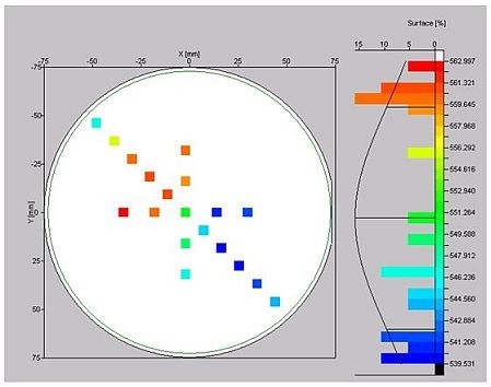
Mercury probe (CV measurement)
- Equipment: Solid State Measurements SSM 495
- Sample sizes: up to 200 mm
- Determination of leakage currents, break through voltages, k-values of insulator thin films
- Free programmable mapping scripts
3ω measurement
- Determination of thermal conductivity (transient hot wire method)
- Simple Aluminium heater structure on the dielectric is used for measurements
- Structure preparation is very easy compared to non-contact methods
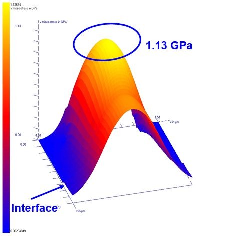
Nanoindentation
- Equipment: UMIS Nanoindentation System (CSIRO, Australia)
- Several indenter types are available: Berkovich, spherical, pyramidical
- Determination of hardness, Young's modulus, yield stress
FTIR
- Equipment: BRUKER VERTEX 80v and BRUKER IFS 66
- Analysis of structural / chemical material properties, for low-k materials in special changes within the Si-O-Si backbone, damage and curing effects, removal of porogens, etc.