 Fraunhofer Institute for Electronic Nano Systems
Electroforming-free memristors for disruptive innovations in AI hardware architectures
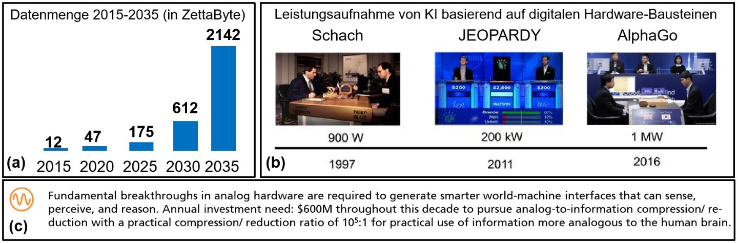
AI with classic digital hardware components based on silicon technology comes up against limits in terms of latency, accuracy, space requirements, data throughput (Fig. 1a), energy efficiency (Fig. 1b), CO2 footprint and learning rate. Those limits cannot be overcome even through the further development of software, or only with extremely great effort. The dimensions of this challenge are described in the latest roadmap from Semiconductor Research Corporation (Fig. 1c).
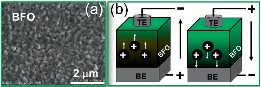
There is a lack of electroforming-free, analog, and digital AI hardware components. Thanks to the electroforming-free AI hardware building blocks BiFeO3 (BFO) memristor and YMnO3 (YMO) memristor, new AI hardware architectures are possible and the potential for a large number of AI hardware-based, disruptive innovations is created.
We rely on a specific infrastructure, cooperation partners and competencies with a unique character: As technology users, this includes SMEs and startups in Germany as well as the local, in Europe unique, Saxon semiconductor industry, which with its structural sizes – Global Foundries 22 nm - have the necessary machinery for production.
In addition, there is the Forschungsfabrik Mikroelektronik Deutschland, software and hardware test beds (TU Dresden, TU Chemnitz, Fraunhofer ENAS) as well as scientists from university and non-university research institutions who are proven experts in materials research for AI hardware, in circuit design and construction, and in AI software development.
We are currently developing AI hardware architectures with electroforming-free memristors for edge computing and for trustworthy electronics in reference projects at the demonstrator level.
Since memristors in highly scalable KI circuits are typically arranged in a crossbar structure, it is generally desirable to use electroforming-free memristors, as otherwise the failure susceptibility of the memristor increases. The electroforming-free BiFeO3 (BFO) memristor (Fig. 2) has all the necessary properties of the missing analog AI hardware component. The electroforming step is avoided in crossbar structures with BFO memristors. In addition, using BFO memristors analog data processing and analog data storage can be integrated as a unique functionality in highly scalable AI circuits. Because of the high variability in the production of BFO memristors, they are suitable for use as PUF crypto-elements (Physical Unclonable Function-PUF) in trustworthy electronics.
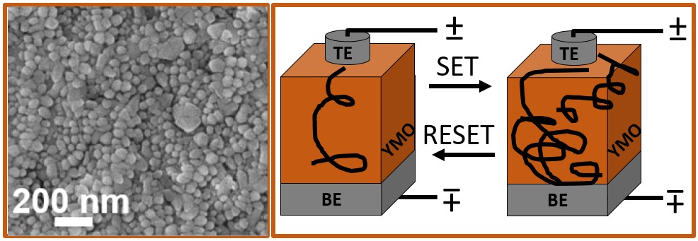
The electroforming-free YMO memristor (Fig. 3) has all the necessary properties of the missing digital AI hardware component and, due to its high entropy, is suitable for use as an RNG cryptographic element (Random Number Generator - RNG).
Based on the electroforming-free memristors, we develop the technology (Fig. 4) for the production of innovative AI hardware architectures for edge computing and for trustworthy electronics. This is the beginning of the 1st seismic shift »The Analog Data Deluge« (Fig. 1c) and represents a new added level of value creation for microelectronics and along their manufacturing process.
.")