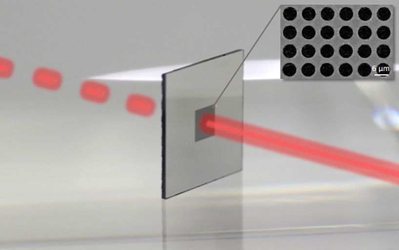
MEMS components with sub-wavelength structures

The use of sub-wavelength structures is an alternative way for functionalizing of optical surfaces in contrast to the application of optical layers or layer stacks. Highly reflecting surfaces, wavelength filtering surfaces, surfaces with extremely low reflectance and highly absorptive surfaces can be achieved. In many cases, only one single layer of a metal or of a dielectric material is applied to form the sub-wavelength structures. Nano structuring by nano imprint lithography opened the way for the commercial application of principles using subwavelength structures and plasmon related optical effects for volume fabrication of these components recently. It is compatible to other processes for the integration into MEMS and MOEMS fabrication technology sequences to fabricate complex MOEMS components. Tunable spectrum filters and shutters are key components of such hyperspectral imaging systems beside of the detector arrays. These novel components can turn infrared imaging into spectral and hyperspectral imaging, which enables to gather substantially more information in comparison to single spot spectrum recording and regular wideband infrared imaging.
 Fraunhofer Institute for Electronic Nano Systems