Cu-TSV for MEMS based on a via last approach


Introduction
Future applications such as mobile devices, wearable electronics, or smart cards have the need to integrate more and more functionality on ever decreasing space. This puts major challenges on the fabrication technology of the implemented devices such as micro-electromechanical systems (MEMS) and their packaging. Here, one widely emerging technique is the three-dimensional (3D) integration based on through-silicon vias (TSVs) and device stacking.
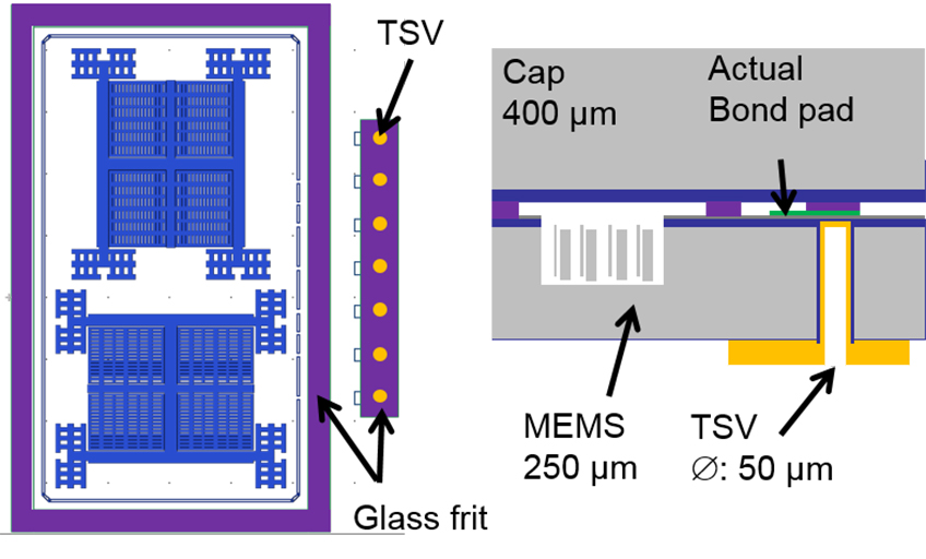
A Via Last approach (i.e. TSVs after wafer bonding) could be applied to the cap of a MEMS device or to its active part. Advantageously, the latter method tolerates intermediate layers (e.g. glass frit bonding). The major challenge is the fabrication of high aspect ratio (HAR) TSVs which results from the MEMS wafer thickness that is necessary to preserve the MEMS integrity and hence, its functionality. This report summarizes the fabrication of a demonstrator based on a two-axis MEMS accelerometer in the so-called AIM (Air Gap Insulated Microstructure) technology as shown in Fig. 1.
TSV technology
The principle TSV process flow (Fig. 2) starts with glass frit bonding (a). In the first TSV process step (b), deep reactive ion etching (DRIE) is utilized to form HAR TSVs with a depth of 250 µm. An LF bias is used to minimize lateral etching at the isolator interface. The buried oxide (BOX) film has to be removed in order to reveal the sensor metallization (c) which is accomplished by a RIE process. As isolation between the TSVs and the bulk-Si (d), a conformal SiO2 liner is deposited by means of a SACVD-based process. This liner needs to be re-opened at the TSV bottom (e). It is realized by a highly anisotropic process that prevents any lateral etching of the sidewall isolation liner and is based on a low chamber pressure for a higher directional ion bombardment.
The metallization (f) starts with the deposition of the TiN barrier/adhesion layers and a Cu-seed layer by a MOCVD process. A photo resist mask is applied and serves as mould for the subsequent conformal electrochemical deposition (ECD) of 3 ... 10 µm Cu. Beside the TSV metallization, the redistribution layer (RDL) is deposited at the same time. After the ECD process the photo resist, Cu seed layer as well as the TiN barrier/adhesion layer are removed (g) by wet chemical etching. Finally, the cap wafer is thinned down from the initial 400 µm to 100 µm by a grinding process followed by a stress release etching in a RIE process.
Results and discussion
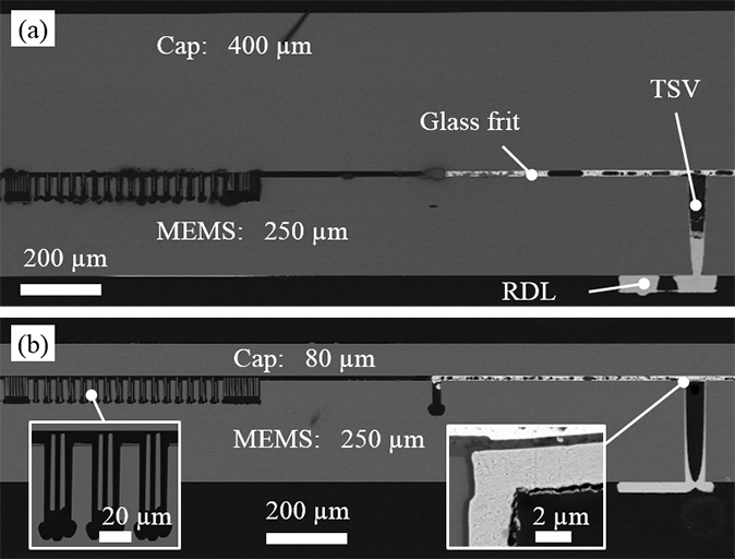
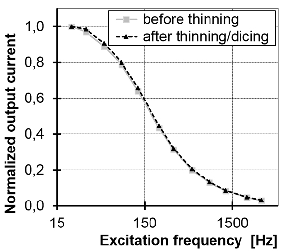
Figure 3 shows SEM images of the MEMS accelerometer with Cu-TSVs before and after thinning to a final device thickness of approx. 350 µm. No grinding or dicing induced defects such as cracks in the cap wafer or in the micromechanical structures could be identified in the SEM images of the thinned MEMS. For the functional characterization of the MEMS accelerometer an electrostatic excitation (sinus with Vpp = 2 V) was applied (Fig. 4). No obvious deviation could be observed between the curves before and after thinning which confirms the functionality of the accelerometer even after the harsh processes of wafer thinning and dicing.
Conclusion
The implementation of Cu-TSVs in an existing two-axis MEMS accelerometer was demonstrated. In the first run, the final thickness of the MEMS yields a value of approx. 350 µm. Further miniaturization in lateral size is possible by adapting the MEMS design to the TSV implementation and further height reduction is currently being addressed by developing a cap wafer TSV technology. Reliability tests will be performed in order to proof the mechanical strength of the complete device and the integrity of the MEMS.
Acknowledgement
The authors like to thank the team of the Fraunhofer ENAS and Center for Microtechnologies (Technische Universität Chemnitz) for carrying out unit processes, cross sectional polishing, and SEM imaging.
 Fraunhofer Institute for Electronic Nano Systems