Direct integration of strain-sensitive field effect transistors for NEMS


Introduction
The drive to more compact and complex integrated NEMS is in need of further shrinking of the transducer elements at the same sensitivity as common used ones. Sensors based on the capacitive principle are scaling with the electrode area and piezoresistor gauge sensors need a certain length of the resistor to get a reasonable sensitivity. An alternative approach is the use of transistors to transduce strain in the channel into an electrical signal.
MOS-Detection for nano size
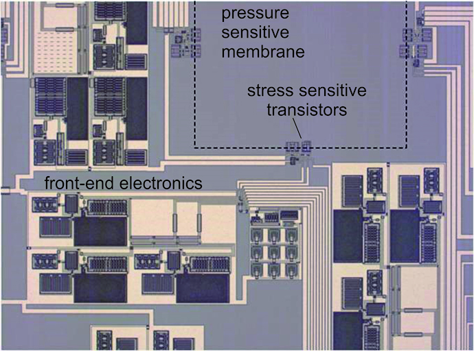
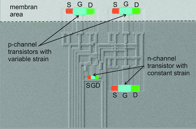
Mechanical stress in the channel of a field effect transistor (FET) influences directly the charge carrier mobility and therefore the drain current and most of the transistor’s other properties. This allows to shrink the transducer size between few micrometers and some hundred nanometers. The manufacturing with a common CMOS process additionally brings benefits to cost, size, sensitivity, signal-to-chip-area-ratio and power consumption. For principle studies on this effect, pressure sensitive membranes with strain sensitive transistors at their edges have been designed and fabricated in a 1.0 µm CMOS technology foundry run.
The strain sensitive FETs are connected in half-bridge mode consisting of two n-channel FETs and two p-channel FETs. It was designed to minimize impact of parasitic effects and temperature on the sensors as well as transferring the source drain current into a voltage, which can be very easily analyzed. In this bridge the p-channel FETs are used as the transducing elements. The source and bulk of the same types of transistors are connected to the input voltage. The drain contacts are connected to create a voltage from the stress influenced source-drain-current. The gate voltages can be controlled separately to adjust bridge voltage directly.
The evaluation circuit is integrated for on-chip amplification, gain adjustment and temperature compensation. This highly integrated system gives the advantage for a temperature measurement on the same chip in close proximity to the active transducer elements. This achieves measuring nearly the sensor temperature which leads to better compensation. Furthermore, the on-chip signal processing minimizes the influences of interconnects.
For design, layout and understanding of the transistor behavior the piezoresistive effect has been integrated into the circuit simulator ELDO from Mentor Graphics®. Therefore, the piezocoefficients of silicon and the stress sensitivity of the charge carrier mobility was added into the model to determine the relation between the mechanical stress and the transistor properties. The complete circuit including the stress sensitive transistors, the amplifiers and the signal processing was simulated to achieve the best performance for the used transducers. For optimizing the position of the transistors in relation to the stress maximum of the membrane, a simulation of the mechanical system has been made using a finite element model.
Measurement results
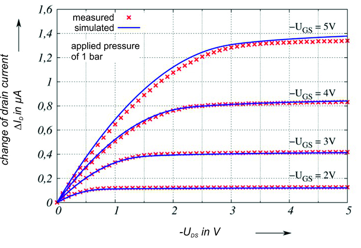
The measurements of a single transistor showed an increase in carrier mobility and therefore in drain current from an applied strain in good agreement with the simulation results. An unamplified gauge factor of 110 could be determined for p-channel FETs, independently of the drain-source and gate-source voltage. The charge carrier mobility was extracted from the transfer characteristic at a drain-source voltage of – 50 mV. Without a stress influence the mobility lies between 190 and 193 cm²/Vs. The current of the reverse biased drain-bulk diode does not show stress influence, but in the breakdown region a gauge factor of 50 is calculated from the simulation.
The Wheatstone bridge configuration shows a linear dependence of pressure changes with 0.64 %-FSO. The test vehicles achieved a sensitivity between 83 and 91 mV/bar with a temperature coefficient of -126 ppm/K. This is a similar sensitivity in comparison to conventional measurement principles with good linearity and low temperature dependence without signal processing. The measured temperature dependence is by factor 16 lower than a conventional piezoresistor strain gauge.
Acknowledgment
This work was funded by the German Research Foundation within the Research Unit 1713.
 Fraunhofer Institute for Electronic Nano Systems