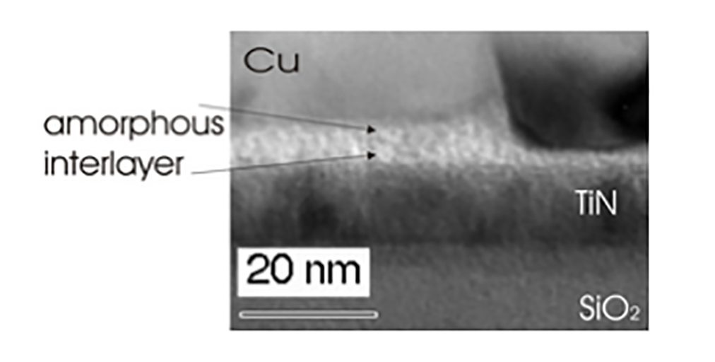
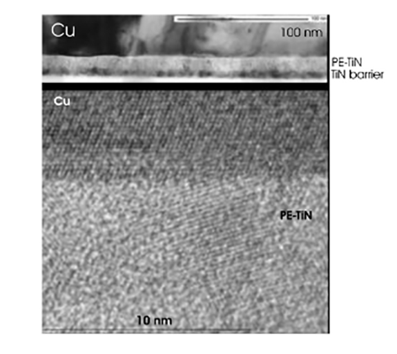
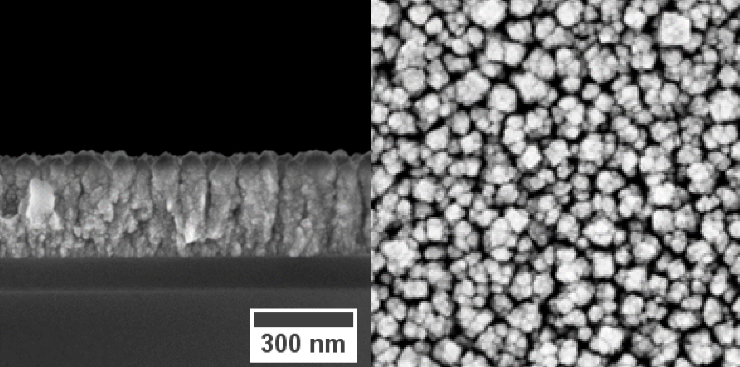
CVD of diffusion barrier: TiN
- Precursor: TDMAT
- Multistep process consisting of alternating MOCVD deposition and plasma treatment steps
- Process optimization for high step coverage with regard to pattern geometry and density
- Stabilization with SiH4 for a better performance of the diffusion barrier, mainly at structure sidewalls
- Deposition of adhesion layer for copper CVD, e.g. for a subsequent CMP process
Copper-CVD
- Thermal MOCVD with CupraSelect™
- Complete fill of structures
- Deposition of seed layers for electroplating
- Metallization of through-silicon vias (TSV): with barrier/ seed for geometries >3 µm; complete CVD fill for geometries <3 µm
- Process optimization for high step coverage with regard to structure geometry and depth, also very high aspect ratios (e.g. >20)
- Metallization of nanometer sized interconnects (<100 nm)
Screening of new metal-organic precursors
- Evaluation of new copper precursors for thermal deposition or reactive deposition
- Testing of other precursors for metal, metal alloy and barrier deposition (e.g. Ru, Sn, Mn)
Equipment
The Fraunhofer ENAS has an Applied Materials P5000™ tool for processing wafers up to 200 mm wafer diameter, equipped with two CVD-chambers (one for Cu-CVD and one for TiN-CVD) and a plasma pretreatment chamber. Both CVD chambers are based on WxZ chambers and have different evaporation systems for liquid precursors, a Bronkhorst system with a liquid delivery system as well as a bubbler system.
Publications
Melzer, M.; C. K. Nichenametla; C. Georgi; H. Lang; S. E. Schulz.: Low-Temperature Chemical Vapor Deposition of Cobalt Oxide Thin Films from a Dicobaltatetrahedrane Precursor. RSC Advances 7, no. 79 (2017): 50269–78. https://doi.org/10.1039/C7RA08810H
 Fraunhofer Institute for Electronic Nano Systems

