Materials and technologies to enable high-temperature stable MEMS and electronics


Modern electronic and mechatronic systems are more and more frequently required to meet harsh environmental conditions while reducing costs at the same time. In many fields of technology, as for example in automotive industry, power engineering, and industrial metrology the high-temperature stability is stretched to today’s limits of feasibility. A further increase of operating temperature is requested to be close to the process of interest but needs new system integration approaches of combining semiconductor technologies, packaging and substrate material development. Within the joint project MAVO HOT-300, various Fraunhofer Institutes worked on extending the operating range of smart systems containing MEMS and electronics up to 300 °C.
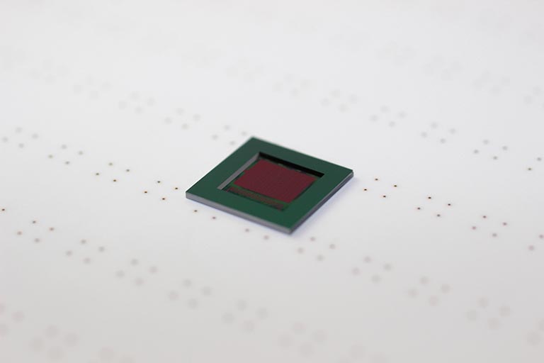
Wafer-level packaged multifunctional MEMS with ceramic interposer
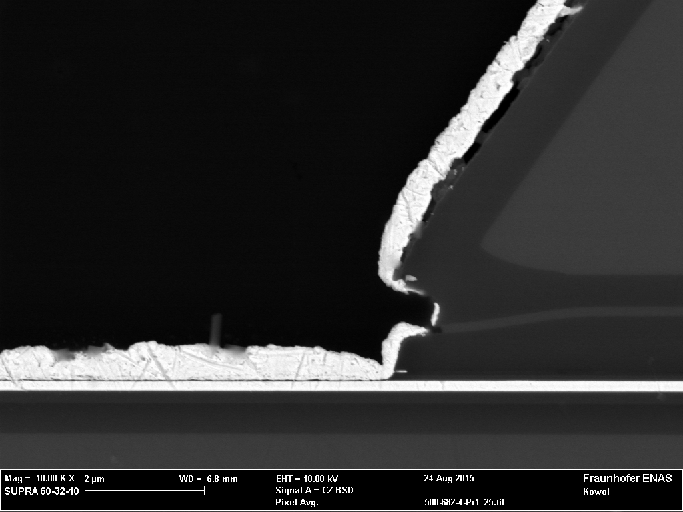
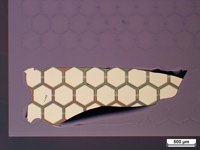
Ultrasonic transducers based on piezoelectric effect are often limited in terms of operating temperature. In this project, we have developed a 1 MHz capacitive micromachined ultrasonic transducer (CMUT) with platinum metallization and integrated temperature sensor on a ceramic interposer. Depending on their size, the ultrasonic cells are also applicable for pressure sensing. A temperature stable composite membrane consisting of thermal SiO2, LP-CVD Si3N4, Ti/Pt and PE-CVD SiO2 has been defined by a combination of sequential temperature-dependent measurements (e.g. layer stress) on the deposited layers together with extensive numerical simulations. This approach leads to temperature-dependent models based on the actual mechanical properties of the deposited layers. The MEMS component is fabricated on two separate wafers, which are assembled by direct bonding of PE-CVD SiO2 layers. To reduce stress inside the package, through-silicon vias (TSV) with thin sidewall metallization between 500 nm and 2 μm instead of completely filled vias are used.
In order to join the MEMS components together with ceramic substrates, a suitable wafer-level bonding technology needs to be developed. As one promising method, the anodic bonding of silicon and LTCC has been investigated. Micro Chevron test was used to determine the bonding strength of the silicon-ceramic interface as a function of bonding temperature, plasma surface activation and testing temperature. To realize electrical interconnections between the silicon and LTCC wafers, thin metal layers are simultaneously thermocompression-bonded during the anodic bonding process.
Reliability and lifetime
High operating temperatures result in new temperature driven mechanisms of degradation and material interactions which are only marginally covered until now. Therefore, the determination of reliability risks and mechanisms as well as their allocation to specific construction situations is an essential part of the research. An operating temperature of 300 °C is considerably above common testing temperatures. In this respect, it is necessary to develop novel accelerated test methods, adjust detection techniques and determine material parameters. The determination of temperature shock strength of electronic components even at high temperatures requires the adaptation of the available equipment. A two-oven system has been developed in which a temperature range from – 70 °C to 450 °C can be covered by using a robotic handling system. The full electric in situ monitoring capability of the samples during the measurement is ensured. Also vibration and humidity can be included in the testing setup within a combined test. With the acquired data, reliability models can be generated and validated which allow reliable predictions and risk evaluations for the new requirements. With combined usage of advanced simulative and experimental methods, it is possible to identify potential weak spots in the overall system. These are, for instance possible interface delamination, determination of fracture and crack risks, ensuring the functionality under changing boundary conditions, evaluation of long-term stability and determination of acceleration factors.
Acknowledgement
This work was supported by the Fraunhofer Internal Programs under Grant No. MAVO 824 712.
 Fraunhofer Institute for Electronic Nano Systems