HyperConnect: self-assembly of micro and nanoparticles by centrifugal forces and capillary bridging for 3D thermal interconnects


Efficient heat dissipation is of major importance in advanced packages of high-performance integrated circuits (ICs). To ensure and extend the integration density, 3D chip stacking with multiple silicon dies vertically arranged on each other is indispensable. However, these packages require an enhanced thermal management in order to dissipate the heat from each stacked die to the heat sink. Therefore, a highly thermal conductive underfill material is essential to affect the thermal resistance of the entire chip stack significantly. Due to the average thermal conductivities of commercially available capillary underfills of ≤ 0.8 Wm−1K−1, traditionally used to relieve mechanical stress from solder balls in flip-chip packages, they are not sufficient for high-performance 3D chip stacks.
The HyperConnect project was a 36 months EU cooperative research project finished in 2015, funded by the European Commission under the 7th Framework Programme (FP7) in the area of nanosciences, nanotechnologies, materials, and new production technologies (NMP) under Grant Agreement no. FP7-NMP-310420. At least 10 partners from Europe were contributing to that project (among others: IBM Research GmbH, Switzerland; Stiftelsen Sintef, Norway; Fraunhofer ENAS, Germany; Technische Universität Chemnitz, Germany).
The goal of the research work was to develop a sequential process flow for an advanced concept of percolating thermal underfill (PTU) using the self-assembly of micro and nanoparticles. Due to the connection of the contact points in a micron-sized particle bed by using nano-sized compound material, a highly percolated network with increased thermal conductive paths was investigated. It was already demonstrated, that the resulting composite material allows thermal conductivities up to 3.8 Wm-1K-1.
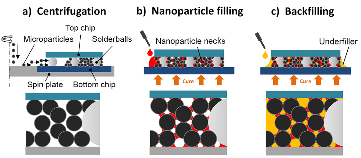
The research work of Fraunhofer ENAS was focused on three main process steps, the centrifugal filling of microparticles into a defined silicon cavity and under a chip-on-board sample to form a percolating particle bed, the self-assembly of nanoparticles around the spherical contact surfaces by capillary bridging (so-called neck formation) and the backfilling of the formed particle network with an unfilled capillary epoxy. Figure 1 shows the process flow.
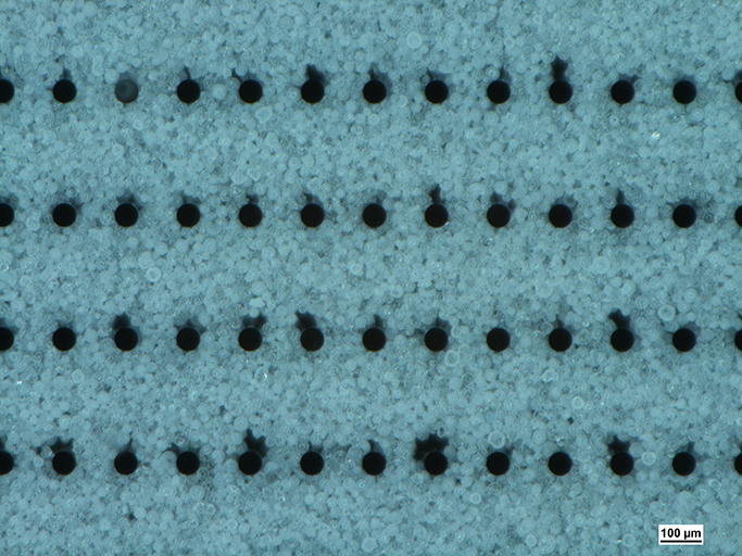
For the centrifugal filling silica and alumina spheres with diameters ranging from 27 to 30 µm resp. 25 to 36 µm, dispensed into a rotating filling disk, were investigated. As a replacement of the solder ball contacts within a chip stack, fabricated silicon dies with different pillar layouts were filled with microparticles. The fill fraction, fill front, packing structure, and occurred defects dependent on the rotational speed were studied. Especially, an empty space in the particle bed behind the pillars in fill direction (referred to as “shadowing”) appeared as a defect (Fig. 2).
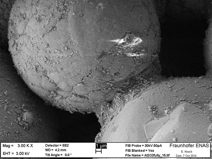
It could be shown how processing aspects did influence the neck formation by capillary bridges between the microparticles. For the initial experiments, metal-based nanoparticle inks were assembled into the contact points of the micron-sized spheres, directed by capillary force during drying. The concentration of the nanoparticle suspension as well as drying and sintering temperatures and times were tested experimentally. In addition, further defects in terms of microparticle rearrangements, voids and air inclusions were examined for different solvents und nanoparticle inks. Finally, the formed particle network is stabilized with a two-component epoxy system (Fig. 3).
The authors would like to thank the colleagues of IBM Research GMBH, Switzerland for their valuable support in experiments, fabrication and characterization. In addition, we would like to thank Kerry Yu from Intrinsiq Materials Inc. for providing the copper nanoparticle ink as well as Albert Aachen from Lord GmbH for the formulation and modification of epoxy matrix material with a low viscosity.
 Fraunhofer Institute for Electronic Nano Systems