Measurement of intrinsic stresses using FIB equipment becomes a method of regular industrial practice


Intrinsic stresses in semiconductor and MEMS devices significantly affect functional behavior and reliability. Trusted knowledge on stress amount and sign is a basic need developing new products. Electronics and MEMS devices often demand an extremely high spatial resolution of stress states. Only a few methods like X-ray/electron diffraction, microRaman spectroscopy, and TEM-based methods have been established as indirect stress measurement tools. Even finite element simulation reaches its limits to predict reliably mechanical stresses, if systems and manufacturing processes are rather complex and material laws are insufficiently known. Stress measurement by means of FIB-based ion milling and subsequent quantification of stress relief deformation is a new promising approach. First papers were published 10 years ago, among them Fraunhofer initial research. Up to now, the method has been utilized and strengthened by several European research labs. Currently, an extensive research program within the European FP7 framework project ISTRESS »Pre-standardisation of incremental FIB micro-milling for intrinsic stress evaluation at the sub-micron scale« is rendered. Its main objective is a commercialization and availability under industrial conditions. Fraunhofer ENAS is one of the consortium partners triggering and executing this program.
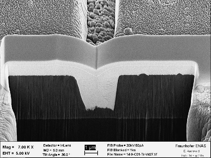
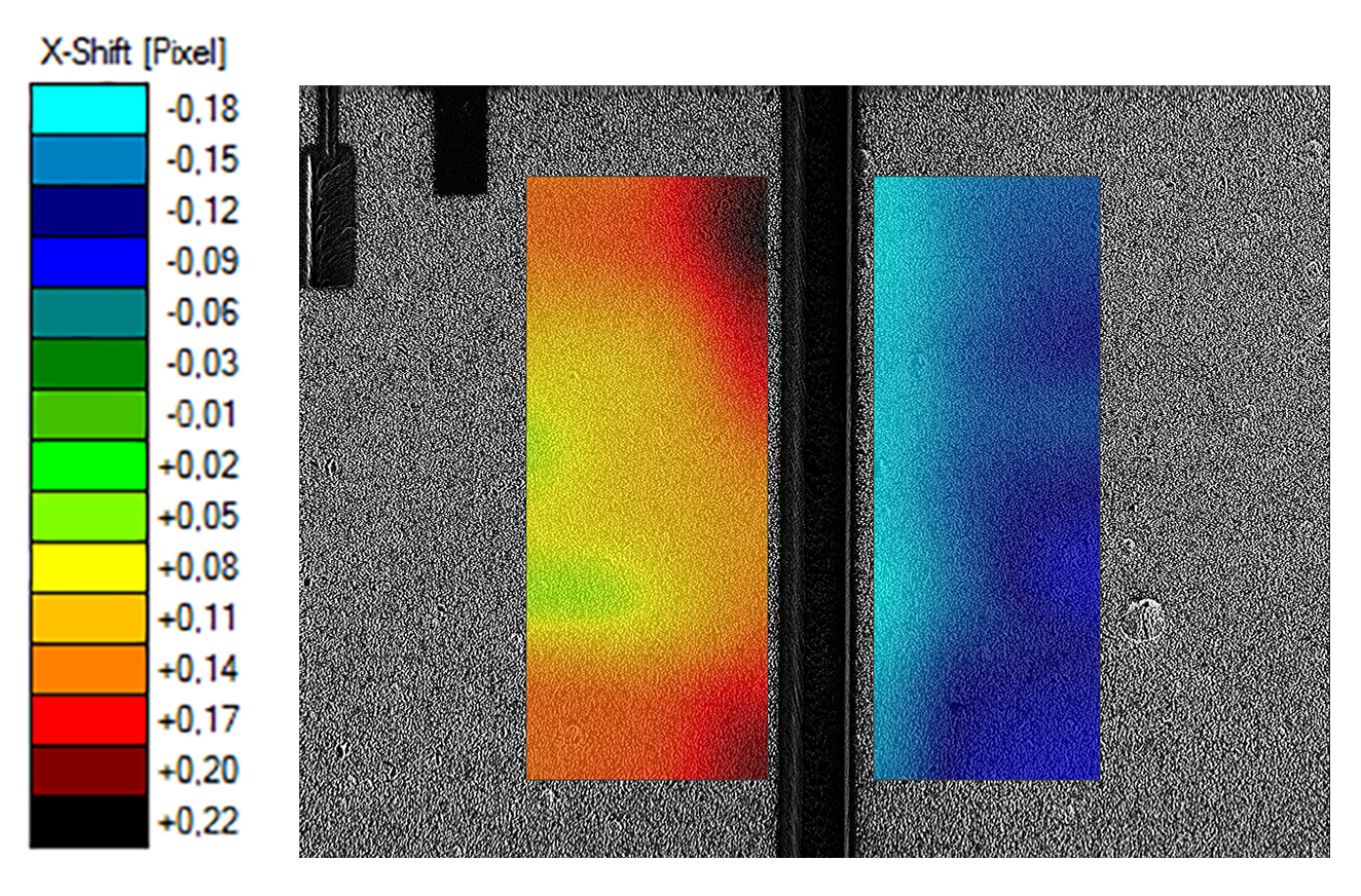
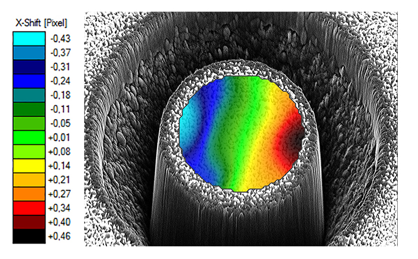
The method, often termed FIB-DIC or fibDAC, uses milling in standard Focused Ion Beam (FIB) equipment to release stresses very locally. Utilizing Digital Image Correlation (DIC) algorithms on high-resolution SEM micrographs captured before and after ion milling, the relief deformation field around the milling pattern is determined. Stresses prior to ion milling are found from measured relaxation strains assuming linear elastic material behavior. Various milling pattern have been deployed in the past, in dependence on the desired stress components and striven for spatial resolution. Some of them are depicted in the Figures 1–3. Typically obtained stress resolution ranges from 1 to some 10 MPa, in dependence on the elastic material properties of studied objects. The method reveals an excellent spatial resolution of 10 nm laterally on patterned surfaces and of 50 nm in depth measurements. Because the method does not require crystalline materials as for established diffraction methods, it can be applied to a much wider group of materials, like nano-crystalline or amorphous materials. The mentioned capabilities make it a favored candidate for local stress measurements on MEMS and electronics products.
In a research lab version, the FIB-DIC approach was applied and tested at Fraunhofer IZM and Fraunhofer ENAS by contributing to different reliability analyses for industrial customers. Nevertheless, the method could not be considered a method for regular industrial use. The mentioned above project ISTRESS tackled this drawback. A designated objective is the automation of the whole measurement process in order to obtain stress results at least within a few hours. Another goal addressed is the creation of a measurement tool which allows cost efficient measurements performed on FIB operator skills. A major European FIB manufacturer (Tescan) joined the ISTRESS project and is looking for implementation opportunities into a commercial FIB system. Beside these activities, the consortium made essential effort to validate the FIB-DIC method aiming at its pre-standardization to reach a wider level of acceptance by industrial users. December 2016, at the end of the project a Best Practice Guidebook will be delivered by the consortium, significantly simplifying access to the tools for new customers as well as giving support for decision makers. The FIB-DIC stress measurement method is not limited to MEMS and electronics devices but addresses many industrial research and development domains faced with stress issues, e.g. for products like wear resistance layers, cutting tools, and high-strength materials for aircraft and power plant engines.
 Fraunhofer Institute for Electronic Nano Systems