High-precision deformation measurements in multi-scale applications – a verification methodology for simulation-based reliability predictions


Electronics reliability and robustness remain in the focus of research
Highly integrated smart systems use in harsh environments remains one of the major trends. Many added functionalities require power and high-power features (e-mobility, direct machine control, energy generation and distribution,…). Hence, the thermo-electromechanical reliability risks will be increased further as compared to the level of today’s smart systems. Another trend is to increase the level of heterogeneity in smart systems integration.
Increased system complexity requires sophisticated modeling
In consequence, the necessity of guaranteeing full dependability and good reliability of the new systems requires systematic research. Thermally induced stress due to thermal mismatch between the heterogeneous systems is generally the source for thermo-mechanical failure. In the field of smart systems addressing the issue of reliability, the physics of failure approach is followed. Efficient virtual design strategies and architectural product features capable of prognostic health monitoring are applied.
Experimental verification of modeling input and output is the key for precise failure prediction
As the levels of packaging integration, material diversity, and system complexity are increased, verification of simulation by experimental means are more important than ever. In particular, highly miniaturized materials used down to the nanometer range imply changes and process dependence of materials behavior, which is hardly to be handled without very special, problem dependent experimental techniques. This is even more important as the increase in integration level may lead to more interlinking and interaction between the different materials.
New optical metrology device allows for precise deformation analysis down to nanometer range in a wide temperature spectrum
The development of a new measuring system for both in-plane and out-of-plane deformations based on a long standing experience in optical measurements for microsystem applications at the department MMC closely interacting with the company Chemnitzer Werkstoffmechanik GmbH (CWM). The need for the development of a new measuring system became apparent after detailed market studies revealed that there is no device in the market which allows for measuring parameters that were targeted for the application spectrum.
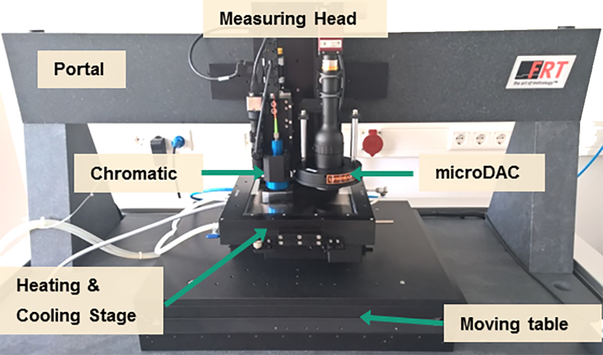
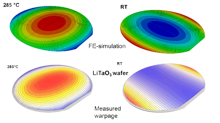
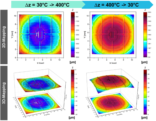
The parameters now realized are really impressive: an out-of-plane measuring resolution of 30 nm and an in-plane resolution of 50 nm in a temperature range between -80 °C up to 400 °C! Obviously, the measuring precision makes sense only in conjunction with a high-temperature stability which is extraordinary as well: 0.01 K controlled by four temperature sensors in the temperature chamber. Field measurements capabilities base upon different measuring principles for in-plane and out-of-plane displacement measurements which are realized as two different measuring heads mounted in such a way as they are able to investigate the same object at a certain temperature. The pointwise measurement of the out-of-plane component is performed by chromatic sensor with a high-precision moving table, both designed by FRT (Fries Research & Technology GmbH) measuring devices. A high-resolution camera delivers the signals for in-plane field measurement of the object deformations. Object deformation at different states is calculated by digital image correlation software VEDDAC which also allows for picture stacking and thereby a limited evaluation of the deformation in the third dimension. An advantage of the measuring system is that measuring precision can be verified by combining the two approaches for the same object. These cases can be used as calibration cases for various objects, starting from the chips or MEMS-level up to the system-level. No doubt that the combination of these measuring system with finite element modeling allows for excellent reflection of the real system.
 Fraunhofer Institute for Electronic Nano Systems